This thread has been locked.

If you have a related question, please click the "Ask a related question" button in the top right corner. The newly created question will be automatically linked to this question.

ADS1271 with the OPA4188

Other Parts Discussed in Thread: OPA4188, ADS1271, ADS1278, TMS570LS1224, OPA188, THS4521, ADS1220

Hi

Im doing a passband filter: high pass 5Hz, notch 60Hz and low pass 520Hz. Then to a summing amplifier to move the signal from 0 to 2.5V. All this with an OPA4188. I was wondering if the ADS1271 could work for me, since it has a differential input... would it work with the AINP on the output of the OPA and the AINN to gnd??

thanks!!

  • Hello Miguel,

    Thanks for your question. The ADS1271 converts a differential input voltage to a digital output by comparing it to a differential reference voltage, VREF = VREFP - VREFN = 2.5V. If AINP was centered around 2.5V, and AINN was tied to GND, the differential input voltage to the ADS1271 would always be ~2.5V, which is basically positive full-scale for the ADC. If AINP was ever greater than 2.5V, the ADC output would be saturated.

    To use the full-scale range of the ADC in a single-ended measurement, AINN should be tied to 2.5V as well. This will allow AINP to swing from 0V to 5V while creating a differential input voltage range equal to the ADC full-scale range (-Vref to +Vref).

    Does that make sense?
  • The signal I will be converting goes from 0 to 5V. Is a miolectric signal to which I already made an offset to move the 0 of the signal to 2.5V so I can get a full positive signal. Instead of having the signal from -2.5V to 2.5V. 

    Thats why i was wondering if it would be fine to connect the AINN to 0V so the comparison be made to the full positive signal...

    Im not sure I understood correctly your message... In I have a signal that goes from 0 to 5V and connect the AINN to 2.5V I will have a comparison of the full signal or how?? How it would work if I have AINN connected to 2.5V?? Would it work as a single input ADC having all the data from the signal converted?? without loosing the data under 2.5 of the original signal?

    im not sure i made myself clear... my english is... well, lets say i need to improve it 

  • Miquel - no te preocupes, tu inglés es mejor que mi español. :)

    Please refer to the figure below:

    As you mentioned, your input signal on INP has been shifted into the range of 0V to 5V. If INN is tied to 2.5V, the differential input voltage (INP - INN) will always be less than the magnitude of Vref (also equal to 2.5V).

    The ADC in the ADS1271 uses the full 24-bit range to convert differential inputs from -Vref (negative full-scale) to +Vref (positive full-scale) and outputs digital codes in two's complement format, like this:

    With a 2.5V reference voltage and INN = 2.5V as well, your input signal from 0V to 5V (INP) will actually use the entire full-scale range of the ADS1271.

    Saludos,

  • Great!! so I just need to connect the AINN and the VrefP to 2.5V right??

    best regards!!

  • Great!! =D

    Hey... two more questions
    1) which can I use to generate the 27Mhz clock source??

    2) What is the usage of the DRDY pin??


    best regards!!!

  • Hi Ryan

    I got a question today... is the AINN like an offset??

    I have a signal (myoelectric signal) and I will amplify it. I was thinking of getting the signal from +-2.5V and putting an offset of 2.5V to move the signal to hae 0 to 5V range. If I dont make the offset, and I only have the signal from -2.5 to 2.5 what could I do to have a full scale range and process all the data??

  • Hola Miguel,

    I'll start with your first two questions:

    1. The CLK input can be generated by a low-jitter crystal oscillator
    2. /DRDY is a digital output from the ADS1278 to trigger an interrupt in the MCU whenever a new conversion result is ready. New data is indicated by the falling edge of /DRDY.

    Back to you questions about input common-mode: 

    The AINN input is not an offset to the signal on AINP. You mentioned that you wanted to shift the common-mode of your input signals to 2.5V. This would allow your signals to range from 0V to 5V, assuming a 2.5V reference and a 5V single-supply.

    AINN should be fixed to 2.5V as well. This way, your differential input to the ADS1278 modulator (AINP - AINN) will always be between +/- 2.5V.

    Best Regards,

  • so... If I understand, the pin will generate an interrupt on the MCU (using pin55 maybe?) and de ADS will start to send the data to the MCU right? Im using the TMS570LS1224

    and about the signal... my signal goes from -2.5 to 2.5 and I was thinking on adding an offset but I was wondering if it would be possible to avoid the offset. But I think the ADC is not capable of receiving negative voltajes on the AINP right??

    Or what could I do to avoid the extra opamp for the offset?? or is easier to use the offset and use the ADC as you told me to before??

    best regards

  • Miguel -

    The ADS1271 input voltage range for each analog input pin is limited to 300mV beyond the supplies. This means -300mV to AVDD+300mV with a single-supply. Therefore, you are correct: AINP cannot go below AGND and you must bias the inputs.

    Typically, the ADS1271 is driven differentially. Take a look at the THS4521. You could drive the (+) input with the output of the OPA188, then use the THS4521 in a single-ended configuration to drive the ADS1271 differentially on a single supply.

    Best Regards,
  • Hi Ryan

    Hope you're doing great. 

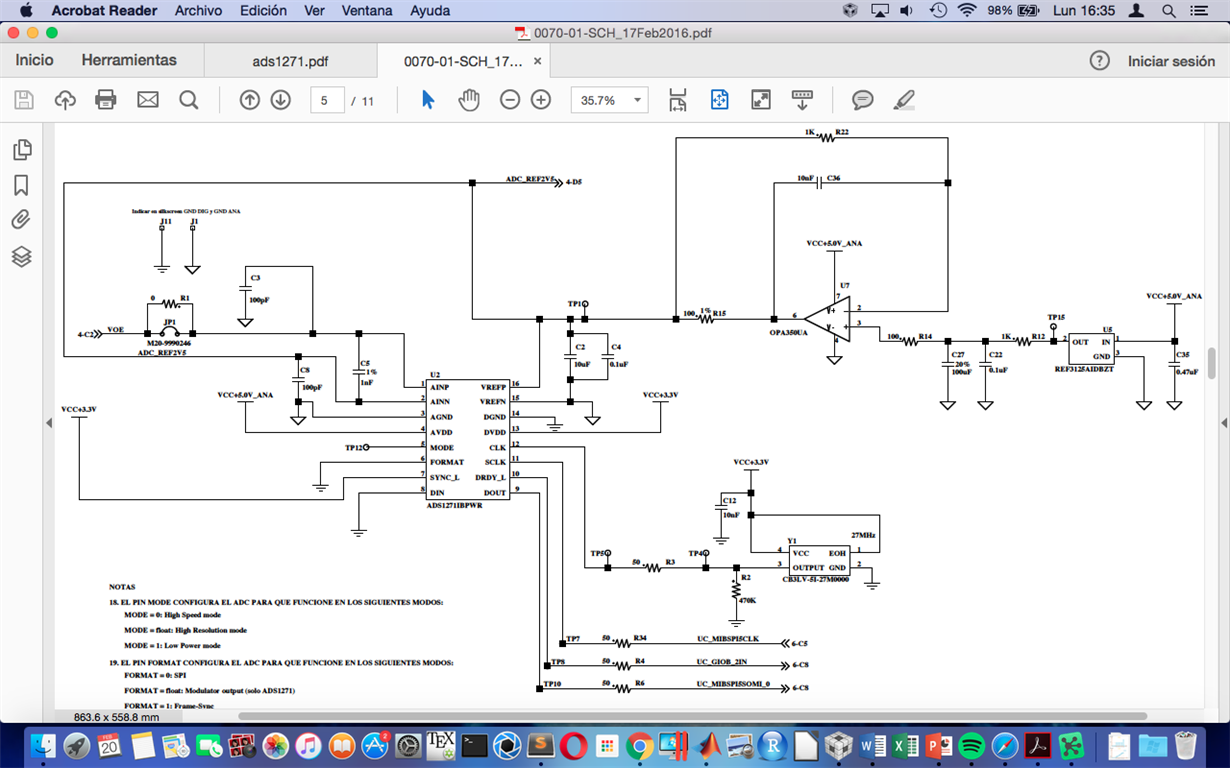
    I already have the board, I just wanted to make sure I understand you correctly and I connected everything as supposed

    Thanks!!

  • Hola Miguel,

    The connections for ADS1271 look correct. Do you have additional decoupling capacitors on the power supplies? Typically you would at least have small, local decoupling caps (i.e. 0.1uF) near the device pins.

    Connections for the interface are ok. You are using High-Resolution Mode and SPI interface?

    What is the DC common-mode and expected amplitude of the signal you are trying to measure on AINP?

    Saludos,
  • amm about the power supplies Im not sure... I don't remember. I took the design from the Hercules launchpad from TI.
    Yep, Im using those two =)

    The signal is supposed to go from 0 to 5V but Im not sure about the range of the ADC output... I'm only sure that after the digital filter the signal is not on the same range, even when the frequency is a low lower than the FIR

    Saludos =)
  • I have a question... the center of the data (vertically) is not fixed right? It depends on the signal amplitude right??
  • The common-mode voltage of the ADC differential output will always be (AINP+AINN)/2. If AINN is fixed, the common-mode voltage will change as AINP changes. We added some new figures to our ADS1220 datasheet that illustrate the difference between a fully-differential signal and a pseudo-differential signal. The latter is what you are essentially doing - AINN is fixed to a DC voltage above ground, while AINP is a moving AC signal. Notice how the common-mode voltage (Vcm) is changing:

    Saludos,

  • Oh... And this behavior is the same on the ADS1271 right?
    So... by having the signal centered on ~2.5 BUT with an amplitude <5, the center of the digitalized signal will vary.
    So I need to make sure my signal always be on the 0-5V scale right? OR calculate the average of the signal, giving me an approximation to the center each time...

    Am I right?

    Saludos! =)