I am trying a "Test Connection" from the Target Configuration on a new board based on the development kit DK-LM3S9D96 (DK-LM3S9B96).
The adapter is a Spectrum Digital XDS100v3 compact TI (CTI) 20 pin dated May 17, 2012. We are using the provided USB cable.
Windows 7
HP 5050 Microtower PC, AMD Athlon II X2 220 Processor 2.8 GHz, 2.00 GB RAM, 32-bit OS
CCS Version: 5.2.0.00069
Settings are:
Texas Instruments XDS100v3 USB Emulator
Stellaris LM3S9D96

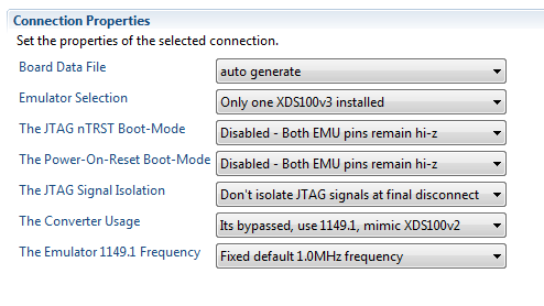
Advanced Settings are default, as recommended by another thread.
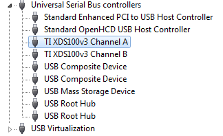
The adapter appears in Device Manager correctly:
We have tried two separate boards, both encounter the same error during "Test Connection":
-----[An error has occurred and this utility has aborted]--------------------
This error is generated by TI's USCIF driver or utilities.
The value is '-233' (0xffffff17).
The title is 'SC_ERR_PATH_BROKEN'.
The explanation is:
The JTAG IR and DR scan-paths cannot circulate bits, they may be broken.
An attempt to scan the JTAG scan-path has failed.
The target's JTAG scan-path appears to be broken
with a stuck-at-ones or stuck-at-zero fault.
[End]
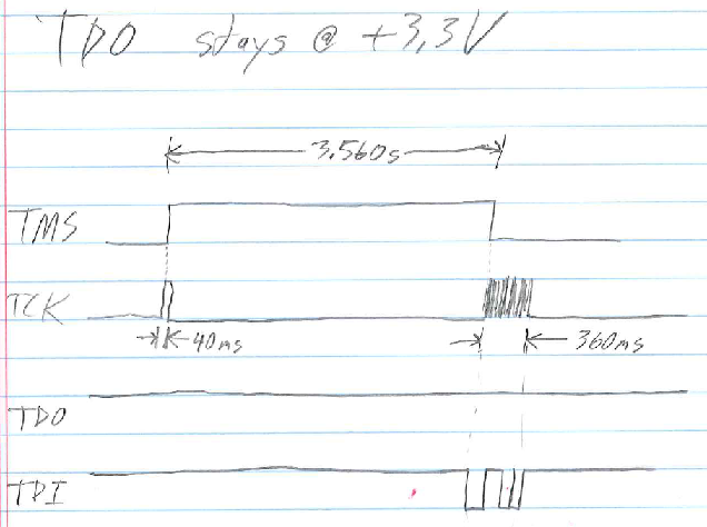
Using an oscilloscope with a needle point, we have taken measurements directly on the Stellaris pins for JTAG. SRST and TMS remain high +3.3 V. TCK is clocking a 3.3 V square wave with a 4 kHz frequency. TDI is also changing state. TDO shows no output. I also ensured the vref is connected to pin 5 as well as grounds on pins 4, 8, 10, 12, 16, and 20
Unfortunately, we do not have a compact TI 20 pin to ARM 20 pin adapter to verify the XDS100v3 is working properly. We are attempting to make one at the moment just to ensure this.
The connections between the Stellaris pin and the pins of the CTI 20 pin header on the board have been continuity checked as well.
What could be wrong?
-------------------------------------------
2012-09 11:37am ET Update:
Ok, we have a CTI 20 pin to ARM 20 pin adapter and have done a successful "Test Connection" with the DK-LM3S9D96 evaluation board. We got the following results:
-----[The log-file for the JTAG TCLK output generated from the PLL]----------
Test Size Coord MHz Flag Result Description
~~~~ ~~~~ ~~~~~~~ ~~~~~~~~ ~~~~ ~~~~~~~~~~~ ~~~~~~~~~~~~~~~~~~~
1 512 - 01 00 500.0kHz O good value measure path length
2 512 + 00 00 1.000MHz [O] good value apply explicit tclk
There is no hardware for measuring the JTAG TCLK frequency.
In the scan-path tests:
The test length was 16384 bits.
The JTAG IR length was 4 bits.
The JTAG DR length was 1 bits.
The IR/DR scan-path tests used 2 frequencies.
The IR/DR scan-path tests used 500.0kHz as the initial frequency.
The IR/DR scan-path tests used 1.000MHz as the highest frequency.
The IR/DR scan-path tests used 1.000MHz as the final frequency.
-----[Measure the source and frequency of the final JTAG TCLKR input]--------
There is no hardware for measuring the JTAG TCLK frequency.
-----[Perform the standard path-length test on the JTAG IR and DR]-----------
This path-length test uses blocks of 512 32-bit words.
The test for the JTAG IR instruction path-length succeeded.
The JTAG IR instruction path-length is 4 bits.
The test for the JTAG DR bypass path-length succeeded.
The JTAG DR bypass path-length is 1 bits.
-----[Perform the Integrity scan-test on the JTAG IR]------------------------
This test will use blocks of 512 32-bit words.
This test will be applied just once.
Do a test using 0xFFFFFFFF.
Scan tests: 1, skipped: 0, failed: 0
Do a test using 0x00000000.
Scan tests: 2, skipped: 0, failed: 0
Do a test using 0xFE03E0E2.
Scan tests: 3, skipped: 0, failed: 0
Do a test using 0x01FC1F1D.
Scan tests: 4, skipped: 0, failed: 0
Do a test using 0x5533CCAA.
Scan tests: 5, skipped: 0, failed: 0
Do a test using 0xAACC3355.
Scan tests: 6, skipped: 0, failed: 0
All of the values were scanned correctly.
The JTAG IR Integrity scan-test has succeeded.
-----[Perform the Integrity scan-test on the JTAG DR]------------------------
This test will use blocks of 512 32-bit words.
This test will be applied just once.
Do a test using 0xFFFFFFFF.
Scan tests: 1, skipped: 0, failed: 0
Do a test using 0x00000000.
Scan tests: 2, skipped: 0, failed: 0
Do a test using 0xFE03E0E2.
Scan tests: 3, skipped: 0, failed: 0
Do a test using 0x01FC1F1D.
Scan tests: 4, skipped: 0, failed: 0
Do a test using 0x5533CCAA.
Scan tests: 5, skipped: 0, failed: 0
Do a test using 0xAACC3355.
Scan tests: 6, skipped: 0, failed: 0
All of the values were scanned correctly.
The JTAG DR Integrity scan-test has succeeded.
[End]
So now we have verified that our XDS100v3 adapter certainly works. We also probed the TDO with the oscilloscope and saw it changing state.
But, we still are at a loss of what could be wrong with our custom board?