A related question is a question created from another question. When the related question is created, it will be automatically linked to the original question.
If you have a related question, please click the "Ask a related question" button in the top right corner. The newly created question will be automatically linked to this question.
Do you have an impedance value for the differential input of CC1120 and I cannot find it in the data sheet and user guide but I can find this value in our previous LPRF IC?
I am engineer at NURI Telecom and developing the module using the CC1120 with CC1190 together.
As the above the question, i can not find the impedance the PA impedance and the differential LNA impedance.
As you can know, when the manufacturers release the RF chip, they must provide the impedance for PA and LNA.
So, i think that engineers who use the CC1120 and CC1190 can develop the RF circuit and fix the impedance for optimizing the RF output and sensitivity.
If engineers don't have the basic imformation provided manufacturer for impedance, they try on and on many times.
And i also think engineers can not debug the RF circuit.
Can you debug the RF circuit without the impedance whether RF chip(CC1120 or CC1190) has malfunction itself or malfuntion of RF componet(for example, mismatching the impedance)???
I think impedance may differ each freqency 170 / 433 / 868 / 915 / 950 MHz band.
Therefore, TI must provide the impedance for PA and differential LNA over 170 / 433 / 868 / 915 / 950 MHz ISM/SRD band.
I and user using the CC1120 and CC1190 do not want to get the simulation value for impedance(30+j30) but get the verified value by measurement.
Please guide the CC1120 and CC1190 for impedance a.s.a.p.
-P.S
I also have another question: does TI have the plan providing the measured data(impedance) to user using CC1120 and CC1190?
if TI don't have the plan and can not provide the impedance, i think engineer won't apply the them on their circuit.
I have been posting on here and even talked with a Texas Instruments Apps Engineer about this and they said they would have to find this out from the chip designers. It does seem strange to me that this was left out of the manual. I have not heard anything back from the chip designers or from the FAE.
But - this doesn't have the information either. It does have placeholders for the information for each band of operation (RX port impedance on page 7 and output load impedance on page 12), but the information is "TBD".
I think this is a vital piece of information which was missed out of the documentation, and I would love to know what it is.
It is common for an amplifier output impedance to be stated at a certain frequency, and it is known that an amplifier output impedance changes over frequency.
So, therefore, since the CC1120 covers many frequencies, the information about output impedance over frequency should be available to designers so they can design efficient matching networks for a given frequency.
Without this information, I'm left to guess. I don't really like guesswork!
We have no plans providing the LNA and PA impedance values. Note that we have never measured these paramenters because our RF reference designs are based on optimal load found by load pull measurements.
Note that the balun chip you are referring to is made for CC1101 and other TI chips that uses the same PA/ LNA. Balun chips designed to be used with CC1120 will be available on the market shortly.
It looks like we're just going to have to tune based upon the reference designs.
Internally we use load-pull and source-pull data to develop the reference designs. It is clear from various posts on the forum that some customers have the need to get additional data to design with our radio circuits.
To get a better understanding of this need could you give me a detailed description on how you would have used the s-parameter data if you had them? This goes for everyone that read this post. From this input we can evaluate if we need to provide more data or a more detailed description on how to use the data we do provide.
We develop the reference designs to help our customers get the best performance possible in shortest possible time. Is it any specific reason you except to have to tune on a design based on the reference design?
Thanks for the response, TER.
Personally, I don't need S parameters, since I don't intend to simulate the design in the classic sense.
Since I don't intend to just copy the reference designs - I would like to see is a graph of PA output impedance over Frequency, or at least the data for optimum impedance in some intended bands of operation (300 to 500MHz, 868 to 869MHz, 902 to 928MHz). I know the reference designs are recommended, but for reasons I can't go into on here I can't just copy them part for part. They won't work for my application.
It is clear from the older version of the data sheet that TI intended to put this data into the datasheet but it never made it there. I think if the information was there, these threads wouldn't exist.
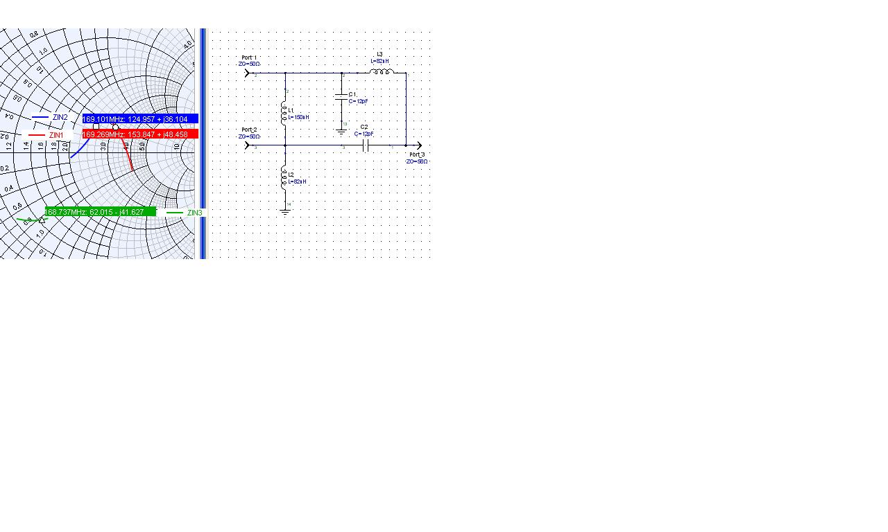
I also need in PA IZout opt. impedance data for the 164-174MHz frequency band. It is necessary for the external power amplifier matching circuit calculation .
If you saw above my post from 19.12.2011 you also may see that output balun impedanse (green line) is far from 50 Ohm and require additional matching for the external antenna switch, which I'm planning to use in my design .
If I use elements 0603 instead 0402 and PCB thickness 1.5mm, impedance also go out from reference design and it needs in correction and simulation.
I agree that optimal load for the different frequency bands should be in the datasheet.
What we have seen in the past is that it is very common to use wrong reference plane when using provided s-parameter files.
One approach is to simulate our reference design using 50ohm ports and when making your own design with different components and PCB thickness aim to keep the same impedances when simulate it in the same way as you simulated the ref design.
Hi guys , here is answer for above disscution :)))
PA circuitry in the CC1120 RFIC is not a conventional power amplifier (e.g., Class A/B/C), it is of a type known as a “switching power amplifier” or “switching power converter”.
- Pout is not a function of the Z load impedance
- Z load impedance must be calculated to obtain Class-E operation
- If the correct value of Z load is provided, the Pout is adjusted by Vdd or by Cshunt at the output of the switching device.