A related question is a question created from another question. When the related question is created, it will be automatically linked to the original question.
If you have a related question, please click the "Ask a related question" button in the top right corner. The newly created question will be automatically linked to this question.
Please follow our reference designs closely, however I can tell you that the output impedance is very close to 25Ohms with not imaginary component to speak of.
We are also in need of s-parameters. Could you share that? I have read in the forum that 2 layer PCB designs with cc2591 may be problematic and may even reduce the performance of the radio module. Is it true?
The CC2591 is a power amplifier and therefore needs good RF ground, we recommend 4 layer designs. Actually, I do not know of any 2 layer reference designs for the CC2591. We do not have s-parameters for the output impedance of the CC2591. Its pretty close to 25Ohm's at 2.45GHz.
Because the CC2591 is optimized for efficiency, it also produces a fair amount of harmonics. Most likely you will be able to "optimize" the output filter to remove any harmonics that might be present on your board after its been manufactured.
Hi Igor Sorry, my mistake. The link is to an internal TI support
forum. I have added the essence of the thread, below.
Hello, A customer has requested S11 data for the
CC2591 in order to design impedance-matching circuitry between the antenna and
PA/LNA. They have also asked to which points the S11 data has been de-imbedded
(i.e., pin, pad, chip, etc).
TheCC2591is
in TX a highly non linear device hence S-Parameters are not accurately
representing the device. TheCC2530_CC2591EM reference design is developed
using load/source pull techniques while continuously monitoring overall
performance such as output power, current consumption, sensitivity, harmonic
content, spurious emissions and more. The reference design is the circuitry
that currently is identified to provide the best compromise of these
parameters. In theCC2530_CC2591EM rev 3.2.1 reference design, the
effective load impedance atCC2591ANT
pin is approximately 13Ω at 2440MHz The impedance is measured by removingCC2591and
measuring the impedance on solder padCC2591pin 11. Note, this impedance is not
necessary the only optimal impedance as impedance on pin AVDD_PA2, AVDD_LNA and
others also influence the effective load/source impedance in normal operation.
This means that i.e. changed AVDD_PA2 impedance can generate different optimal
ANT pin impedance measured on pin 11. Remember that impedances at other
frequencies also influence circuit operation. Especially the filtering
characteristic holds dramatic influence on overall circuit performance. The differential impedance
between RF_N and RF_P whenCC2591is
terminated as in reference design is approximately (105+J30)Ω at 2440MHz OptimalCC2530load
impedance forCC2530is
approximately (69+J29)Ω Given the complexity of
dependencies inCC2591designs
we recommend copying a reference design as closely as possible to minimize the
number of design iterations necessary to get acceptable overall performance. Tor-Inge
Thanks Tor! I will forward this info along
with AN086, AN068, and the CC2530-CC2591EM Ref Design. Also, while we will
definitely suggest that the customer follow the reference design as closely as
possible, making modifications only to accommodate changes in board thickness
per AN068, etc., do we have some load-pull and source-pull data (e.g., in the
form of a Smith Chart, etc) that we can also share with the customer since that
said that they would also like to run simulations if possible? Regards,
Hello Tor, The customer has
built a simulation model and has asked if we can confirm the complex impedance
that should be seen on pin-11 looking back into the CC2591 and with the antenna
removed. They are simulating 28+j13, and have asked if we can confirm that they
are close or need more work. In your previous email you had said that the
optimal load impedance at the CC2530 was 69+j29. Similarly, what would the
optimal complex impedance be at the CC2591 output? Regards,
Measuring the impedance on p11
intoCC2591will
as previously mentioned depend upon the impedances connected to CC2591on
AVDD_PA2 and AVDD_LNA and will hence hold some variation from design to design.
The optimal load on CC2591 p11 (ANT) is measured to approximately 13ohm, no
significant imaginary part. The impedance is measured atCC2591pin11
on theCC2530_CC2591EM rev 3.2.1,CC2591 removed and the RF signal routed to SMA
(through 0ohm resistor) and the SMA terminated with 50ohm. On other designs with different
impedances connected to AVDD_PA2 and AVDD_LNA this impedance might be different
we have seen load impedance values up to around 30ohm generally with a small
inductive imaginary portion. Based on this a load impedance of (28+J13)ohm seem
a realistic value. Measuring impedance into pin 11
will provide varying results dependent uponCC2591mode
(TX, RX, PD), supply voltage, measurement power (network analyzer test signal
amplitude) and AVDD_PA2 and AVDD_LNA impedance. Tor-Inge
Removing CC2591 from CC2591EM, measuring impedance presented on PIN ANT result in close to 33+J7 ohm.
On CC2591EM the differential impedance between RF_N and RF_P is close to 105+j35 when CC2591 in TX and ANT connected to 33+J7 (CC2591 re-soldered onto the board.)
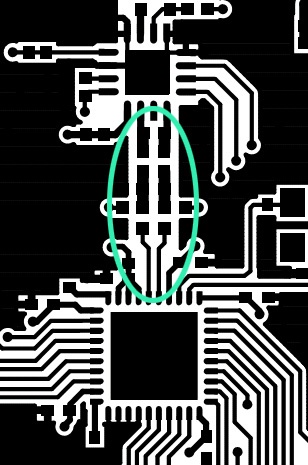
In the "CC2530_CC2591EM reference design" the input to cc2591 the "Complex Impedance Matching Networks", is very long. see photo 1. And has 7 component's between cc2530 and cc2591. that may be good for reference design, but in the real world , it take too big PCB space, and make it near imposable to use the cc2591 if this PCB space must be wested.
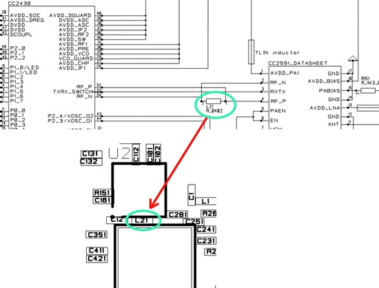
In demo reference design cc2430 and cc2591 it use only one coil, see photo 2. Can we use this reference design? and we can use only one coil between cc2530 and cc2591?
I read in some RF guide paper, that : "If Traces Shorter than 1/20th λ Long, Zo Matching is usually Not Important. "
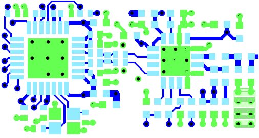
I see you point, however the output stage of the CC2430 and CC2530 are so different that the same match could not be re-used. Here is a layout study we did not show that a compact layout can be acheived with a CC2530+CC2591 device. The match between the CC2520 and CC2530 is the same.
Thank you for the excelant PCB space saving example.
Can you share with me also the Gerber file of this design with it's PCB stack up, PCB material (Dielectric Constant, loss Tangent, Copper Conductivity), so we can imitate that 100% to get same RF result ? (maye also RF tests also ...)
I would like to build wireless project use cc2500+cc2591.I have known output impedance (RF-N -- RF-P) of cc2500 is 80+j74 and input impedance of cc2591 is 105+j35. So need to matching them.Use the Smith chart, i build matching circuit as the picture. I got VSWR for cc2500+cc2590: 1.14, VSWR in output is 1.07. IS this working good and properly?
I would highly recommend you to use the CC2592 (http://www.ti.com/product/cc2592) instead of the CC2591. It is easier to work with and will give you better performance.
Is CC2591 NRND yet? I'm trying to get our customer to switch to CC2592 but he says, "changing the part now has too much risk." However, they haven't gotten the CC2591 to work yet, either. If the CC2591 were marked NRND it would be much easier to get them to switch to CC2592. Thoughts?
CC2591 is not NRND but we recommend CC2592 for new designs since this is a improved version of CC2592. Could you repost on the internal forum with more details about what their problem is?
Their problem is that they are way behind schedule, their prototype (having many flaws) based on '2591 is badly mistuned, and they have little RF expertise or equipment. They are renting equipment and I'm training them how to use it, but I think we would all agree it would be much easier to use '2592.
Not sure what else to add, if I need more help I'll contact you internally. If you are still interested, look me up.
As far as possible they should follow the reference designs for CC2592. Then the design should most likely work out of the box and no extra tuning is needed.