This thread has been locked.

If you have a related question, please click the "Ask a related question" button in the top right corner. The newly created question will be automatically linked to this question.

BQ76940: BQ76940

Part Number: BQ76940
Other Parts Discussed in Thread: TIDA-00792, BQ76200, TIDA-00449, BQ76920, BQ78350, , BQ78350-R1

Hi,

In  BQ76940 evl board reference schematic, battery each cell is  connected  to BQ76940 IC though resistor,capacitor & mosfet has a switch.

1) what is the use of connecting the battery each cell to BQ76940 IC though resistor,capacitor ? resistor and capacitor used for filtering?

2) P mosfet work has a switch for External passive cell balancing through 100 ohm resistor ? and 100 ohm resistor load?

3)can we use P mosfet instead of P mosfet?

Regards,

Rajaneesh

  • Hi Rajaneesh,

    1. Yes, the resistor and capacitor are used for filtering.  It is important to keep transients on the battery out of the inputs of the IC.  Exceeding the ratings of the IC can result in damage.

    2. Yes, the P-channel is a switch to provide higher balance current than is allowed by the filter network.  100 ohm is used for the balancing load on the EVM.

    3. Yes N-channel balance FETs can be used and may be preferred.  See the application notes and reference designs associated with the part in the bq76940 product folder Technical documents tab and Tools & software tab.  The application note bq769x0 Family Top 10 Design Considerations and TIDA-00792 may be particularly helpful.

  • HI,

    Thank you for your quick replay,

    1)      External passive cell balancing is mandatory? Should I use in my design? Or only RC filter is enough?

    2)      Which cell connection is best for cell balancing?, with P-channel FETs or N-channel FETs?

    3)      Please brief me on mosfet (FETs)specifications (lithium ion battery Pack voltage 48V & 15A current)

  • Hi Rajaneesh,
    1. External balancing is not necessary, but internal balancing current is low. If the cells are good and the system is cycled frequently the low current may be fine. Also be aware of the the dIALERT load on the bottom cells. If the system leaves ALERT high most of the time there may be a 15 uA load on the lower cell group. There should be some example balancing discussion on the forum.
    2. Either one works. I would suggest N-channel since it avoids the stress on the inputs during cell connections.
    3. The protection FETs operate as a load switch type application. They will be on most of the time, protection should be rare but the FETs must switch reliably when used. Since it is normally on a low RDSON is generally attractive to avoid heating the battery, but cost and system design for heat removal are considerations. It is common for batteries to see a 2x voltage transient in batteries, so a FET with a 1.5 to 2x of the battery voltage rating is a common choice. The FET may go into avalanche to clamp the protection transient. You don't need the FET to switch fast as with a switching regulator application, too fast of switching will excite the cell inductance at high current. You do want the FET to switch within its safe operating area. Hope that helps, you might check industry references on FETs or with your preferred supplier. TI does offer FETs, consider the products and information at www.ti.com/mosfet.
  • Hi,

    Our design specification 48V 25A (lithium ion battery)

    Kindly clear my below queries.

    1)How to select balancing load Resistor ? its depends on load,how much we draw? R=V/I R=3.6V/28.7E = 125mA , is that right?

    2)C22 must be GND?

    3) Mosfet is enough for CHG & DSG ? or need to use bq76200 CHG and DSG High-Side NMOS FET Drivers?

    4)Can i use parallel mosfets for CHG & DSG for high current? kindly suggest for our design

    5)Bq76940 is supported for 48V 25A?

    6) how do i select External cell input capacitance?  in datasheet given 0.1uF to 10uF. shall i use 0.1uf or 0.22uf?

    7)how to select RSNS resistor?Using the normal max discharge current, RSNS = 200 mV / Peak Discharge Current = it will be in mΩ

    is that correct? in why they mentioned 0.001 ohm in reference design?

  • Hi Rajaneesh,
    1. Yes, ohms law. Consider the FET resistance if it is significant, and the power in the FET for the current. You will want a FET with RDSON at low VGS. CSD13381 has a RDSON specification at 1.8V.

    2. C22 should be connected to GND, it was not on some of our references and they have worked, but GND is recommended.

    3. Low side MOSFETs will work if you have an isolated communication path. If you want a communication referenced to PACK- you will likely want a high side switch.

    4. Yes, paralleling MOSFETs is common for higher current or to spread heat. See TIDA-00449 for an example with low side. See the bq76200 applicaiton note on FETs. The drivers either low side or high side have internal resistances, so switching will with more FETs.

    5. Yes, the bq76940 responds to voltages, currents are supported with selecting the sense resistor. Obviously the dynamic range is limited.

    6. The data sheet has range values for the bq76920 to bq76940. With smaller input resistors for the bq76920 you may want a larger capacitor. For the bq76940 you will typically want the smaller capacitors. If you have low transients, use the 0.1uF, if you expect larger transients use the 0.22uF. You could try the larger value and if you have voltage artifacts with balancing you might change to the smaller ones.

    7. You have to pick something in the dyamic range of the part and consider the power in the sense resistor. The data sheet has a simple example in 8.2.2.1. This may be more specific to your situation:
    The maximum OCD value you can set is 100 mV, see the Protect 2 register. Keep tolerances in mind, if your 25A is continuous, you might select 75mV as a desired sense input voltage at your 25A which will not trip. 75mV/25A = 3 mOhm. This would be your maximum resistance. At 25A a 3 mOhm resistor will dissipate 1.875W. If you can tolerate this power on your board you might select resistors and use this value.
    If you use a 1 mOhm sense resistor, 25A will give 25 mV. There are several settings above this for OCD so you can select the threshold so it always passes. Power in the 1 mOhm at 25A is 0.625W, selecting a resistor or resistors may be easier. The other thing to consider is the 8.44uV resolution of the CC. With 1 mOhm you will have a resolution of 8.44uV/1mOhm = 8.4 mA. If you want a higher resolution you will want a larger resistor.
  • Hi,

    Please find the attached schematic,Kindly verify the schematic & let me know if i missed out anything or any further modifications.

    Schematic designed for 13s pack 48V 2.5A

    Battery pack 48V 25A  13S10P  

    Please clarify below queries.

    1) Below mentioned charger adapter is enough for charge battery? 

    Charger adapter: 48V 3A CC / CV / Float Constant voltage

    2)What is the input for REGSRC? is it  works for 48V or 37V? datasheet says max 25V/36V

    3)Can i read the data of BQ76940 , BQ78350 through I2C from micro controller?is that possible?

    4)How should i communicate or read/write data of BQ78350 through micro controller?should i interface through SMbus?or can be communicate through i2c?

    5)FET mosfet are enough for control CHG & DSG? or should i use BQ76200PWR?

    6)Can i tie  the #DISP pin  to VSS if i am not using the LCD? BQ78350 pin no. 14 #DISP

    Thank you

    awaiting for your favourable reply

    Regards,

    Rajaneesh

    BMS_8.pdf


  • Hi,

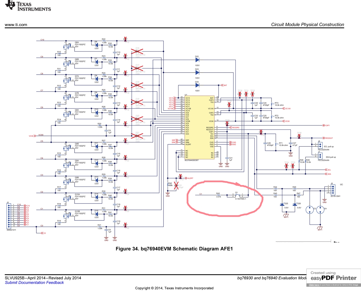
    I didn't understand the concept,which i have marked in red color in below schematic & the attached schematic from bq76940EVM ,tidrqy7.

  • Hi Rajaneesh,
    The bottom of C31 should go to GND as you have connected, but the right side of R55 must connect to VC0 for balancing.
    The ESD zeners to PACK- will not work, D28, D29, D31, D33, when the system protects with load PACK- will go to PACK+ and push current into the bq78350 damaging the IC. You need these referenced to BATT-. SMBC and SMBD will need to reference GND also, if going out of the battery you may need an isolated communication path or high side switch. A high side switch approach is shown in TIDA-00792.
    The TIDA-00792 circuit circled is an electrical method to boot the part when it has been shutdown, it provides a signal to TS1 when PACK+ ramps and the system is off. The switch on the EVM is a manual or mechanical boot mechanism, the user must push the button to boot.
  • Hi,

    Please find the attached updated schematic,Kindly verify the schematic & let me know if i missed out anything or any further modifications.

    1)PACK+ Boot Circuit is mandatory use?

    also waiting for your reply on above queries

    ------------------

    1) Below mentioned charger adapter is enough for charge battery?

    Charger adapter: 48V 3A CC / CV

    2)What is the input for REGSRC? is it  works for 48V or 37V? datasheet says max 25V/36V

    3)Can i read the data of BQ76940 , BQ78350 through I2C from micro controller?is that possible?

    4)How should i communicate or read/write data of BQ78350 through micro controller?should i interface through SMbus?or can be communicate through i2c?

    6)Can i tie  the #DISP pin  to VSS if i am not using the LCD? BQ78350 pin no. 14 #DISP

    -------------------------------------------------------------

    Kindly verify the attached schematic

    BMS_ Schamatic.pdf

  • Hi Rajaneesh,
    You will need to be certain of your schematic. I don't see any problems but you must be sure.
    1. You must have a way to boot the bq76940. If it is not booted it will not work.
    1. CC/CV charger is common. You should be able to configure the gauge to terminate so that the continuous charge voltage is not present to the cells.
    2. REGSRC is a power supply input. It has a limited range compared to the BAT pin. The part would be very happy with a 15V regulated input but it is more normal to provide a voltage drop from battery+ with a circuit shown.
    3. I2C and SMB are similar, see the specifications for details. I2C can go to DC, SMB cannot. MCUs can usually support both with the same peripheral
    4. The bq78350 uses SMbus.
    6. DISP is an input and should not be left floating. A pull up is recommended when not used. Connecting to VSS would make the input active if you are not in LCD mode, I would not recommend this.
  • Hi,

    1)What voltage & current need to select? for charging the 13S10P lithium ion battery.

    The voltage should be 54.6V for charging 13S10P?  (Each cell max voltage 4.2V)

    2)what and all controller can read/write from the BQ78350 through SMbus?kindly find the attached block diagram.

    controller can read OV,UV,OCD,SCD etc,all controller can read the data from the BQ78350?controller will have full access to read?

  • Hi,

    Awaiting for your valuable reply on above queries.

    Thank you

  • Hi Rajaneesh,
    1) Select a charger appropriate for your cells. Consult your cell data sheet and/or your cell supplier. Yes, 13 x 4.2V is 54.6V
    2) Any MCU which supports SMBus protocol should be suitable to communicate with the gauge. It should have access to all registers in the bq78350-R1. See the technical reference manual section 16 on communications and 17 for commands.
  • Hi,

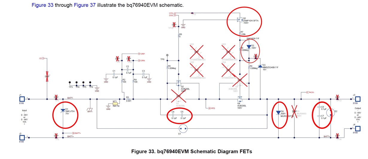
    Please reply on my queries on BQ76940EVM schematic slvu925b.

    1)what is the functionality of C4,C5?why we need to use that?

    2)what is the functionality of C6,C7?why we need to use that?

    3)D1 & D4 used for protection?please explain

    4)what is the use of Q5?can we connect CHG directly to R7 ?bypassing Q5 

  • Hi WM5295 ,

    kindly reply on above queries.

    Regards,
    Rajaneesh
  • Hi Rajaneesh,
    1) C4 and C5 provide a low impedance path across the FETs for ESD current. 2 caps are used in series so that if 1 shorts the FETs are not bypassed.
    2) C6 and C7 provide a low impedance path across the PACK terminals for ESD current to avoid it all flowing into the circuitry. Again 2 are used in series to prevent a direct short if one fails.
    3. D1 is a TVS to help clamp inductive response of cells to fast current turn off. D4 is a flyback or freewheel diode to prevent PACK- from rising much above PACK+ when the discharge FET opens.
    4. Q5 allows the gate of the charge FET to fall below VSS so that the charge FET remains off when there is a fault and a charger is connected to a low voltage battery. Without Q5 the charge FET could operate as a source follower with high enough voltage difference and allow continued charge of the battery. See the bq76940 data sheet 7.3.1.3.1 and figure 7-3.