This thread has been locked.

If you have a related question, please click the "Ask a related question" button in the top right corner. The newly created question will be automatically linked to this question.

LM3450A 340us Off-Timer

Other Parts Discussed in Thread: LM3450

Hello!

I built a Flyback Power Supply (24V, 26W) with orientation towards http://www.national.com/an/AN/AN-2150.pdf
I used the LM3450A:
http://www.national.com/ds/LM/LM3450.pdf

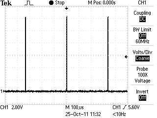
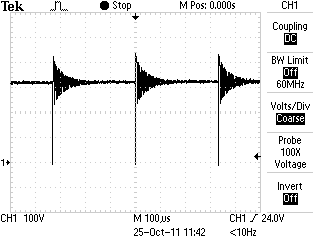
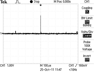
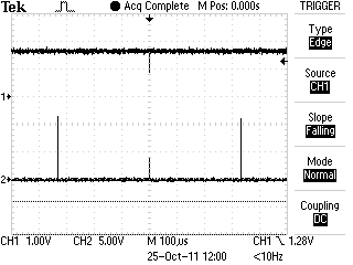
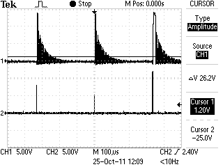
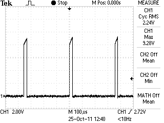
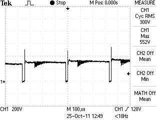
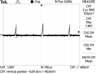
Now my problem: The Power Supply stays always in the mode, where every 340us a short impulse comes over the GATE-Pin, then another 340us the MOSFET is off and then trys to switch again and so on. Can you please tell me all cases where the LM3450 changes to this "max. off-time" mode, so I can validate why my circuit stays in this mode all the time?

The 340us are the max. Off-Time (normal operation) of the LM3450A-Off-Timer (datasheet).

Has anyone similar problems using the LM3450A?


Thank you very much!
Kind regards!
Thomas Huber

  •  

    Thomas,

    Your LM3450 application must be in burst mode when you see the 340us off-times, meaning COMP voltage is below 1.4V. 

    This could mean that the output power is so low and/or the switching frequency is so high that the minimum duty cycle (caused by leading edge blanking) is providing too much energy to the output.  COMP continues to fall far enough (<1.4V) to force burst mode where one on time occurs followed by the max off-time.  This continues until COMP rises back above 1.4V nominal (+ hysteresis).

    The other possibility is that the ZCD (zero crossing detection) is not wprlomg properly.  If the voltage at the ZCD pin does not fall below ~1.24, then the correct off-time will not occur and eventually a maximum off-time will occur.  I'm not sure why this would be happening but you can probe the ZCD voltage to check.


    I can look at the circuit in detail if you can post schematics, relevant operating points (input voltage, LED stack voltage, LED current, etc..), and (if possible) operating waveforms showing the burst mode.

    James Patterson

    Staff Applications Engineer

    Texas Instruments

  • Hello James,

    thank you very much for your reply!

    I put the Scematic in the appendix and I will provide the waveforms later the day, when I can measure again.

    I also put the data of transformer construction in the appendix.

    The operating points are: Vin = 230V, 50Hz; Vout = 24V; Pout = 26W. I use only the first stage, so there is no LED Driver at the Moment.


    Thank you very much!

    Best regards!

    Thomas Huber


    5280.Schematic.pdf

    1680.transformer construction.pdf

    Note: in Scematic, I put more MosFETs etc. in it to get flexible footprints. As output capacitence I only use one 680uF.
    For Clamp Circuit i used the left path in scematic and for Q1 and Q3 i used the suggested ones from the app note (STD4NK80ZT4 (Q1) respectively SPD06N80C3 (Q3)).
    Also I use only one transformer. Instead of two parallel 1R resistors, I use three parallel 3R resistors for "R30||R31" (other current limitation setting, higher power disipation possible).

  • Hello James,

    here comes the first wave, which shows waveforms under no load condition:

    Voltage directly on Gate-Pin of Switching-MosFET Q3.


    Voltage Drain-Source of Q3.


    Voltage over shunt "R30||R31". During the measurement a overall resistance of about 1 to 1.4 Ohm was installed (no 0R5 like in scematic).


    COMP-Voltage (CH1) and Gate of Q3 (CH2).


    VZCD (CH1) and Gate of Q3 (CH2). The Cursor shows the 1.2V mark of VZCD.


    Thank you very much! Scopes of load conditions will follow.

    Kind regards!

    Thomas Huber

  • Hi,

    like I promised here are the load-scops:

    Voltage directly on Gate-Pin of Switching-MosFET Q3.


    Voltage Drain-Source of Q3.


    Voltage over shunt "R30||R31". During the measurement a overall resistance of about 1 to 1.4 Ohm was installed (no 0R5 like in scematic).


    COMP-Voltage (CH1) and Gate of Q3 (CH2).


    VZCD (CH1) and Gate of Q3 (CH2). The Cursor shows the 1.2V mark of VZCD.


    The load is a 33R resistor whereas the output voltage breaks down to 12V under this load condition.


    Kind regards and many thanks for your help!

    Thomas Huber

  • Hello!

    Has anyone a idea, what could cause the Burst-Mode? Maybe the transformer does not fit?

    Suggestions are thankfully welcomed!


    Kind regards!

    Thomas Huber

  • Hello,

    has really no one any idea?

    Do I have to provide additional information to allow resoving the problem?

    Kind regards!

    Thomas Huber

  • Hello,

    after some further trys the board is still unable to leave the burst mode.

    Kind regards!

    Thomas Huber

  • Perhaps is too late, but I had the same problem for 24V power supply.

    Comp voltage stays fixed at 4.7V. Regulation did not work, output voltage fixed at 21V.

    Chip was damaged. Replaced the chip and everything worked properly.

    Stefan H.