Hello,
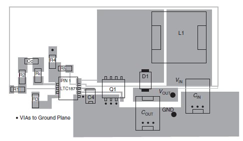
I have made a prototype boost converter (on strip board) using the MSP430 as the controller, i have a RC snubber over the switch (following the SLVA255 - Minimizing Ringing at the Switch Node of a Boost Converter guide) but was wondering how i should layout the snubber in the PCB design. The following picture shows a suggested layout for a boost converter. I'm using Altium designer for the PCB design.

I'm pretty sure that the values of R and C will need change so i was thinking of just leaving some 1206 footprints open on the board and adjust the values when i populate and test the PCB.
Should i put the R and C footprints on the underside of the board or just as close to the drain and source terminals of the NMOS as i can get??
Thanks
Michael Dalton

