This thread has been locked.

If you have a related question, please click the "Ask a related question" button in the top right corner. The newly created question will be automatically linked to this question.

TPS63020 excessive ringing during switch cycles in boost mode

Other Parts Discussed in Thread: TPS63020, TPS63020EVM-487

My customer needs to fix their issue below ASAP:

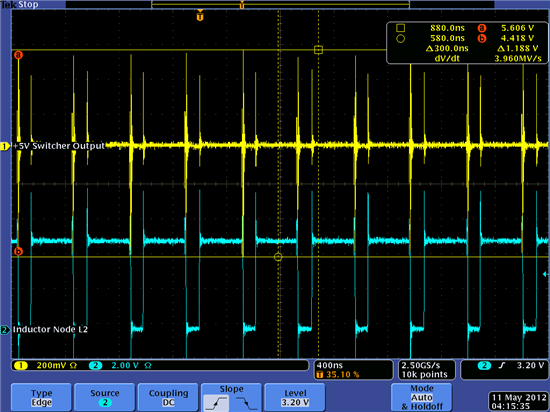
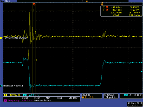
We are now in the process of doing validation testing on the hardware for this project. We have a new issue with the TPS63020 power supply chip and we could use some help from TI. The problem we have is excessive ringing during switch cycles in boost mode with the supply. Power Save mode is off so the device is in continuous operation mode. I have attached some scope traces that show the output. Since we are operating in Boost Mode (3.0 to 4.4V input, 5V output), I expect that the primary contributors to the overshoot are the two FETs connected to inductor node L2. The other two FETs should be continuously ON or OFF at all times during operation.


I have been looking at using a snubber circuit to damp these oscillations, but I would like to know a few things:


1) What is the expected parasitic capacitance of each of the power FETs? This would help me get an estimation of the capacitor I need to use for my snubber.


2) I have never designed a snubber for a synchronous boost switcher before. I assume that I need to consider the combined parallel capacitance (and associated inductance) of the two switching FETs in my design. Can you confirm this to be the correct approach?


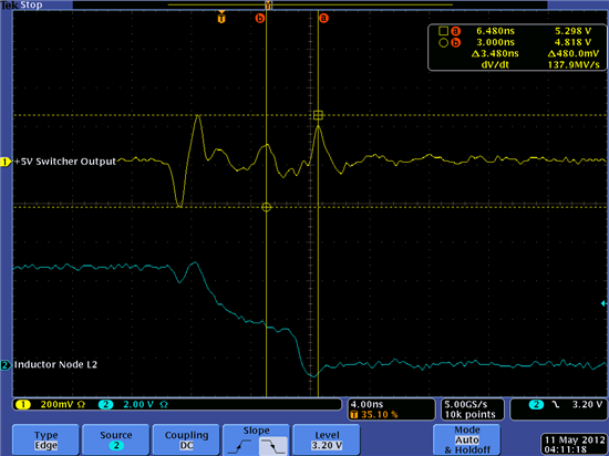
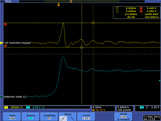
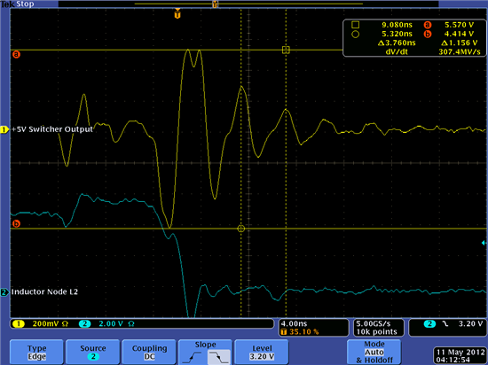
3) I have attached some scope traces of the output ringing in conjunction with the switch voltage at node L2. The output noise was measure with an active probe and a very low inductance ground lead (1.5cm). I observe that the oscillation at the switch point is significantly worse when the L2 node is being switched to GND (falling edge) as compared to the rising edge. Is there an explanation for this based on the switching operation? I assumed based on duty cycle that the current through the FET to GND is higher than the current through the FET to output.

Switching Noise at +5V Boost Output

Rising Edge Unloaded

Falling Edge Unloaded

Rising Edge with 500mA Load

Falling Edge with 500mA Load

Thanks!


  • I am the customer that originated this post. I can add some additional information as I have made some progress on this problem. 

    First I can detail the input/output conditions and the most important components:

    Vout = +5V, Vin = +3.0 to +4.5V, Iout = 2.0A max

    L7 = Coilcraft XAL4030-332MEC

    C567, C569-C571 = TDK C2012X5R1C226K

    I went through an iterative design process to create a snubber between the L2 node and ground. I ended up using a 1000pF cap and a 3R3 resistor. This circuit is somewhat effective at damping the oscillation on the rising edge of the switching waveform. However, it does not damp the ringing on the falling edge of switch waveform. This situation seems to be noticeably worse under load as opposed to unloaded.

    If you look at the scope trace below, you can see that the ringing at the rising edge is significantly reduced with the snubber installed. It is feasible that additional tuning could further damp this. The problem is that the snubber has not effected any change in the frequency of the oscillation on the falling edge. This has me questioning whether I understand where the ringing on the falling edge is originating.

  • This may be more an issue of your design being on the verge of instability. Please try decreasing the value of the inductor to 1.5uH. The datasheet is in the process of being updated to reflect known-good inductor/capacitor combinations. 

  • We tried reducing the inductor value to 1.5uH. This value is technically below the design guidelines for our output voltage.

    The results show worse performance with the 1.5uH inductor, especially at high currents. First we show the performance with the 3.3uH inductor as originally designed.   We measured the switching waveform at node L2 (designated LX in the scope trace) and the output voltage on the 22uF bypass caps near the +5V Output (designated VBUS_OUT).

    Ringing voltage with 3.3uH inductor and 500mA load

    Ringing voltage with 3.3uH inductor and 1000mA load

    Next, we measured the same nodes with the 1.5uH inductor installed:

    Ringing voltage with 1.5uH inductor and 500mA load

    Ringing voltage with 1.5uH inductor and 1000mA load

    To summarize, here are the measured ringing voltages:

    3.3uH Inductor: 270mV @500mA load, 228mV @1000mA load

    1.5uH Inductor: 294mV @500mA load, 331mV @1000mA load

    Note that we removed all snubber circuits to make this comparison simple.

    It seems that the inductor is having a minimal effect. If we look at the period of the ringing waveform it is as low as 3.8ns (corresponding to 260MHz). This is well beyond the resonant frequency of the inductor. This seems like a switch resonance more than instability. I expect instability to be manifested at lower frequencies. Can we rule out instability as the root cause?

  • Which design guidelines are you referring to? If the converter can operate with a 3.3uH inductor, you will need > twice as much output capacitance as with the 1.5uH. You currently only meet the output capacitance spec for the 1.5uH. 

  • From TPS63020 datasheet:

    L2 = Vout *0.5 * us/A  (3)

    L2 = 5.0V * 0.5 = 2.5uH minimum

    We chose 3.3uH.

    Cout = 10* L uF/uH = 10 * 3.3uH *uF/uH = 33uF  (6)

    We have Cout = 3x 22uF = 66uF which is twice the required minimum. Parts are rated at 16V.

    DC bias effect will certainly reduce the effective capacitance amount. However, if stability was a major factor, I would have expected the 1.5uH inductor to improve it. We have a stable DC output voltage and we do not observe any large variations in the input voltage. Our symptoms seem limited to the high frequency ringing during switch transitions. Do you still suspect instability? 

    I will add an additional 22uF to the output to verify whether bulk capacitance is the issue.

  • I believe you have an older version of the datasheet. The datasheet was re-worked due to issues of this type, mainly regarding under specified output capacitance. Also, are you testing on the EVM or the customer board? If customer board, will you please supply your layout?

  • I checked the latest datasheet and there are changes which I will work through. In the Output Capacitor section the recommendation is to use a typical value of 30uF. No other specific information or formula is given for what is required for stability. Is there more information available on this? 

  • We are about to spin this PCB so I am supplying you with our latest and greatest layout. Here is the latest schematic:

    Here is a section of the layout. I have labeled most of the critical parts.

    Please provide any feedback you might have.

  • Have you been able to duplicate this issue on EVM?

    Where are the feedback resistors? These traces need to be as short as possible and should be laid out like the TPS63020EVM-487 as should the rest of the components and traces.

    Your output caps are too far from the output pins. Your input and output ground loops need to be on the top layer. It is recommended to fill the gaps between the sets of pins that are connected together. 

    Additionally, there is still not enough output capacitance for the 3.3uH inductor. I tested L2 and VOUT in the lab on the EVM, as is, with 3V in and 1A out, and measured less than 100mV of ripple on the output.