This thread has been locked.

If you have a related question, please click the "Ask a related question" button in the top right corner. The newly created question will be automatically linked to this question.

Leading Edge Blanking problem with the TPS40210

Other Parts Discussed in Thread: TPS40210

Hello:

I'm designing a 500V to 15V, 0.75W flyback converter using the TPS40210.

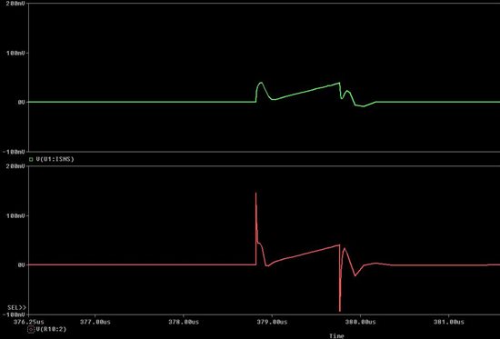
Because the input voltage is high and the power is low, the current going into the switching MOSFET's drain is small, and the current coming out of the source is significantly influenced by the gate current.

As a result,  I'm getting a rather large square wave imposed onto my current waveform. Because the square wave is so big, I can't really filter this out with a simple RC filter, so I have to rely on the leading edge blanking in the TPS40210 to ignore it.

My problem is the pulse is around 170ns and the datasheet gives a typical blank time of 75ns. I tried lowering the gate resistor, to drive the MOSFET faster (IRFBF20) but it didn't seem to help much.  I suppose I could find a lower gate charge mosfet (IRFBF20 is 38nC) or a faster one, but I'm already a little worried about putting too fast of an edge on such a large voltage.

Does anyone know a good way to deal with this problem?  Is this really a problem?  The circuit seems to work in the simulator but I'm worried that when I build it, it will be erratic because it may respond to the hump at lower current commands and to the end of the ramp at larger current commands.

I attached some waveforms from my simulation.  The red is the voltage at the sense resistor, and the green is at the ISNS pin after my RC (499-ohm, 75pF). The hump is around 170ns wide.

  • Patrick,


    As the lead applications engineer supporting the TPS40210 controller I can tell you that it is a real potential problem and an unfortunate implication of the design of the TPS40210 controller in applications such as yours where the peak inductor current will be very low.  In applications such as these it is possible to observe the PWM comparator triggering on the "bump" rather than the peak and the duty cycle alternate very very short (triggering on the gate drive pulse) and long (triggering on the peak current when it becomes large enough)

    Something that will help is the internal slope compensation of VDD / 20 per switching cycle.  Without knowing your switching frequency or VDD voltage, it's hard to know how much benefit this will add during your 1us ON time, but it will help.

    As an example:  With a VDD of 12V and switching frequency of 100kHz, the ramp is 600mV (12V / 20) and the ramp rate is 60mV/us.  The current sense gain is 5.6, so the effective slope compensation to a 1us pulse width with be 10mV on the current sense wave form.  This would then scale with frequency and VDD.  If the VDD voltage is 24V and the switching frequency 300kHz there's 6x as much slope compensation during that same 1us, so whether this will be an issue in your application will depend on both your switching frequency and your VDD voltage.

    A couple of other things you can do to help this:

    1) Increase the time-constant of the Isns filter to 1/3 of the minimum ON-time

    2) You can also add a very small coupling capacitor to force Isns low when the switch turns on (switching node is driven low).  This coupling capacitor connects from the switching node (MOSFET Drain) to the ISNS node and will form a divider with the Isns filter capacitor.  The capacitor should force no more than 50mV change on ISNS voltage at maximum drain voltage.  so Cblank = 0.05V / Vsw(max) * Cfilt

    For 500V on the drain and a 75pF Cfilt this would come to 7.5femto, so you'd need to increase Cfilt significantly to make this a reasonable capacitor value.  For a 10pF blanking capacitor to work with a 500V drain voltage, Cfilt would need to be 100nF, so that ising going to work well.

    We could emulate this effect by connecting a secondard FET to BP with a 10k resistor.  This will produce an 8V square-wave in time with the switching of the main FET and draw less than 1mA of current from BP.  A coupling capacitor would then need to be less than 1/160 of the Cfilt capacitor.  Cfilt would still need to be increases, but 1000pF at Cfilt would allow a 6.2pF blanking capacitor.

  • Pete:

    Thanks for helping me out again.  

    From your suggestions with the slope compensation, it seems like lowering the sense resistor would also help because it increases the ratio of the slope compensation to the current sense waveform.  I'm going to look into making sure that's as low as the design can live with.

    Also from your discussion, it seems like I could use a larger coupling capacitor as long as I shrink the square wave.  In other words if I add a resistor in parallel with the secondary mosfet, I could significantly scale down the square wave, allowing for a much larger capacitor. Is there any drawback to doing this? I realize that I'm adding a pole/zero combination to the original RC filter but I'm not sure that would have a negative effect. 

    I experimented in the simulator with scaling it way down to less than 100mV so I could use the same size cap as a coupling cap, and it seemed to work, except that I was getting a charge injection problem. The charge from the gate would force a brief spike on the drain which carried through the coupling cap to the Isns pin.  Changing to a BJT instead of a mosfet seemed to fix that.

    Can the TPS40210 be damaged by very brief spikes up to say 0.8V lasting for a few ns on the Isns pin?

    Also, why do I need to limit the correction to 50mV?  Could I momentarily force the pin slightly negative?  In the simulator the shape of the correction pulse and the problem pulse don't line up really well (I think it's because of the leakage spike in the main waveform) so it would be nice if I could force it a little below zero to say -50mV for a few ns. Would that cause a problem to the IC?

    This is the current waveform I have in the simulator. Green is at the sense resistor, and the red is at the Isns pin.

    I still have a residual hump in the corrected waveform, but I had to drive it negative at the very beginning.


  • The pin is rated to -0.3V, so it's not a problem forcing it to -0.05V isn't a problem.  My concern with the 50mV was actually focused on the terminal edge when the same circuit results in an increase in the ISNS voltage, though from your simulations that doesn't seem to be as much of a problem as I was thinking it might be.  It looks like we've worked out a fairly effective way to add external leading edge blanking to the circuit.

    Spiking the pin to 0.8V could be more of an issue as this could potentially trigger the PWM comparator since the 0.8V signal would be driven through the current sense amplifier and if the output of that amplifier (likely driven to saturation) can't recover before the blanking period ends, every pulse terminates on the 800mV spike.

    Also, if the OCP circuit hasn't recovered before its blanking period ends, every spike triggers OCP and thus shut-down of the converter.

  • Thanks again.  I believe this is now a workable solution. 

    Just as an FYI, I found that adding a resistor in series with the coupling cap allows you to shape the correction pulse, essentially spreading it out more.  The result is an even better looking waveform at the Isens pin (i.e. the red waveform). Almost no negative spike and a very small hump

    Thanks


  • Patrick,


    Thank you very much for your work on this.  I am certain that many customers will be able to benefit from this circuit design technique for improved current limit and regulation when constructing circuits where the gate drive current is comparable or even greater than the peak switch current.  This type of design collaberation and sharing is the heart of the TI Engineer to Engineer forum.

  • Hi

    Was is possible to "attach" schematic as I'm working on flyback on TPS40210 circuit where blanking issue might be of concern. (or generate app note on this design issue).

    I have 24V to 35V I/P voltage with +/-14V O/P based on flyback. The O/P current is minimum 10mA to 150mA. I would like to set clock to 300KHz to keep circuit compact as possible, and wondering if Peter experience issue when using higher freq.

    Richard.


  • Here's the schematic

    Q1 and Rsns, Rfilt and Cfilt are all part of the standard TPS40210 circuit.

    Q2 switches with the main switch to inject a small current into the current sense and blank out the gate drive current from the rising edge of the current sense signal.

  • Thank for the schematic....

    Apart from Rsns and Q1, do you have typical value and Q2 PN to recommends?

    Wondering why TPS40210 lacks blanker cirrcuit like MAX771 (now discontinued)

    I'm running on +/-14V (+/-100mA) O/P flyback with VIN = 15V to 35V. The Q1 has very low QON, CISS. I running on 300KHz.

    R.


  • On 2nd thought........

    With I/P voltage actually less than 35V, do I need this blanker modification circuit?. The guy mentioned 500V which is why the spike is larger than 35V

    What you think Peter?


  • Richard,


    The key issue is not the input voltage amplitude, it's the upto 500mA of gate-source current during the turn-on of the MOSFET passing through the current sense resistor.   Since the TPS40210 uses current mode control, if the gate drive current is greater than the peak switch current, the PWM control can trigger on the gate drive current rather than peak switch current, causing instability.

    For low current applications from lower voltages, a gate drive resistor can reduce the gate drive current and prevent this issue.  At higher voltages, the switch would be too slow if the gate drive current was reduced below the peak switch currents, so we needed to come up with an alternate solution.


    As for component sizes, you are producing a capacitive divider with Ccouple and Cfilt, and you want to produce a negative pulse to mask the gate drive current - so you want to force ISNS down by 500mA * Rsns.  If you size Ccouple = 1/10 Cfilt, you'll need to size the resistor divider to give you 11x Rsns * 0.500A at the midpoint of the divider

  • One note - the way the schematic I drew is connected, you'll need the smaller divider resistor between BP and Rcouple and the larger resistor from Rcouple to the MOSFET such that the Rcouple voltage is VBP - 11x Rsns * 500mA when the MOSFET is ON.

    You could flip the two resistor values by connecting the divider directly to ground and moving the MOSFET's drain to the Rcouple location - but this increases the power dissipation of the injection circuit.

  • This is my schematic.  I used a divider to ground and a BJT to reduce charge injection.