This thread has been locked.

If you have a related question, please click the "Ask a related question" button in the top right corner. The newly created question will be automatically linked to this question.

LM2678-12 Load Problem

Other Parts Discussed in Thread: LM2678

Dear TI,

We are trying to desing a switching circuit with the LM2678-12 IC with these caracteristics:

Input Voltage: 20V-32V

Output Voltage: 12V

Output Current: 5A.

The Webench designer, says that i have to use these circuit:

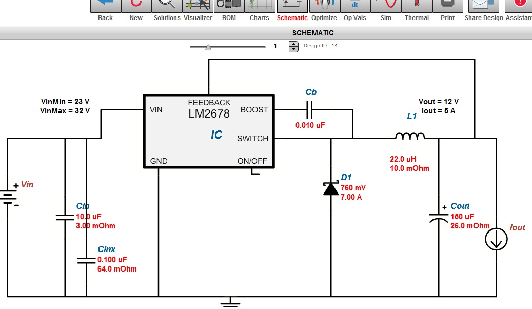
The components usead were those recomended by webench designer.

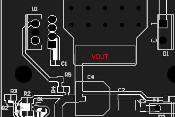
Making reference to the desing of the circuit, the power diode and the Cb are close to the IC.

The problem is that we put the load @ 4A (3 Ohm aprox) the Output voltage fallsout of range to 10V or 11V.

Measuring with the OSC the inductor signal with a low resistance load, we saw that was a ringing that probably affects the circuit stabilization, so we put a little capacitor (47nF) in parallell with the power diode, the problem was solved but the capacitor starts to heat too much (because of the low ESR).

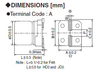
One thing that we notice is that the recomended power diode (http://www.vishay.com/docs/94249/6cwq06fn.pdf) consists of 2 legs (3,5A each one) and when we put the to legs to ground the circuit falls to 10V when the load is 3A. So we tried connecting only one leg (to reduce the junction capacitance) and it works well untill it reaches 4A.

Other thing is that the tables of the Application note of the LM2678-12 IC, says in the Figure 23 that for an input of 25V and 5A of output we need an inductor L49 of 33uHy, and its different to the webench recomendation (22uHy see circuit).


With all these problems we dont know why the circuit doasnt work, any information to solve these problems is grateful.
Thanks.

  • Hi Ariel,

    A Couple of questions.

    1) Can you share your board layout?  Routing of the input capacitors to the ground connection of the diode and the input pin of the device is very important for device operation.

    2) What output capacitor did you end up using and what are its parameters?


    Regards,

    Marc

  • Marc, first of all thank you for the fast respones.

    1) The layout is the one in the pdf, before any correction, want you to know that we made modifications while were testing this circuit, because we notice that some components are too separate, so we put them closer (not in this design of the pdf, but in the real circuit that we were testing). The power diode is closer to the IC, as the input capacitor Cin, and the Vsw node (inductor, diode and IC pin) were closer too.

    2) The output capacitor (Cout) we end up using is the one with PN: APXA160ARA151MJ80G


    Regards.2818.DOC_P0712PCBFSW01_INFORMACION ARMADOR.pdf

  •  

    Hi Ariel,

    1) Looked at the output capacitor.  The specification look fine, but when I look at the datasheet and compare to your layout, it looks like the capacitor is placed backwards on the layout.  It appears that the negative terminal is connect to Vout.  Can you check this?


    2) I can't find the 10uF input capacitor on the layout.  Can you highlight the component number or where it has ended up in your experimenting.  The routing of this capacitor to the diode and the part is the most important to have well layed out in a buck converter.  The capacitor ground needs to be right next to the diode ground and the Vin connection of the capacitor needs to be as close as possible to the Vin pin of the part.


    Regards,

    Marc


  • Marc,

    1)The Cout silkscreen is badly drown, but in the real circuit its well placed, i think it would have exploded if I connect it wrong.

    2)The input capacitor of 10uF is C2, i will modifiy the circuit to achieve that C2 ground is as close as posible to the diode ground and de positive terminal to Vin of the LM2678.

    We are in contact,

    Regards.

  • Marc,

    We tried to put the input capacitor next to de IC and the ground next to de ground of the diode and we achieved 5A with 11.8V, so i supose its working ok.

    Regards.

  • OK Good.

    Now if the output voltage is dropping at full load, that is probably because of the sense point of your feedback divider.  It is sensing the voltage right next to your output capacitor.  Your output trace extends past this, and if you are measuring somewhere else in the circuit you might be getting resistive losses which are lowering your voltage.  So a good check is to see what the voltage is directly at the output capacitor.  If this is 12V then you need to either increase the width of the 12V trace (or make a plane if possible) or take a trace from where you want the 12V regulated back to the top feedback resistor.


    Regards,

    Marc


  • Actually, I built a 24V in 12V out LM2678S-12 demo circuit exactly as the WEBENCH assembly drawing indicated.  I ran into two problems:

    1.  The PCB I ordered was the correct part number, but did not match the actual assembly drawing generated online.  It was close enough that I could make it work, so I continued.

    2.  Once built, with component placement nearly exactly per the pdf, I experienced the same problem identified in this thread.  It turns out that the Cin in the sample circuit is about 1.25" away from the switching diode.  It is nowhere near the input pin either.

    When I connected a generic 10uf capacitor (leaded) between the diode ground and pin 2, the circuit voltage stabilized, just like the comment above indicates should happen.  This suggests that either the evaluation PCB layout is sub-optimal, or the assembly drawing is in error.  I suspect that using a low ESR cap between pins 2 and 4 of the regulator might work reasonably well, but there is very little room at that location (nothing larger than a meduim-size chip cap will fit). 

    I suggest you update the online simulation to prevent others from having the same problem.


    Thanks,


    Paul