Other Parts Discussed in Thread: ISO1541, , TCA9517, PCA9306, ISO1450, P82B96, ISO1640, TCA9517A
I have a design that requires isolated power supply to two sections (let's call them section A and section B). We have I2C running from section A to section B, which I would think needs to be buffered. The TCA980x family was recommended, so I was thinking I would power Vcca = section A's 3.3V, and Vccb = section B's 3.3V, and GND = ground B.
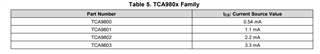
I need some help with how to select which TCA980x device to use, as well as how to size the pull-ups.
The I2C bus is running at a 400kHz frequency, and we only have one device on it (i.e., one master controlling one slave), so following the estimation of 15pF bus capacitance per device and looking at the limits for each device, is it correct that any of the TCA980x devices should suffice, regardless of the rise time? I ask because I'm not entirely sure how to determine what the rise time is. The FPGA documentation doesn't spec a rise time (I'm also not very familiar with FPGAs so I don't know if that's something that's usually specified or not).
Since the pull-up resistance is also calculated based on rise time, is it best to size the pull-ups assuming a really fast rise-time so that I don't accidentally exceed Rpmax for whatever the rise time actually is?
Additionally, there are pull-ups between the FPGAs and bus switches. Are the existing 10k pull-ups sufficient or do pull-ups to the 3.3V supplies need to be added prior to the TCA980x buffer?
Thanks for your help.