A related question is a question created from another question. When the related question is created, it will be automatically linked to the original question.
If you have a related question, please click the "Ask a related question" button in the top right corner. The newly created question will be automatically linked to this question.
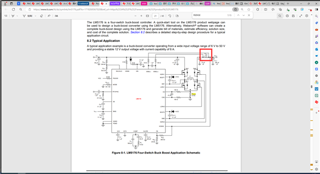
LM5176:The problem of ground short circuit of the pin of the low side FET control stage on chip
As for this chip, I tried switching from boost mode to buck mode after soldering. I found that my chip was not working directly after the switch, and the pin of the low-side FET was short-circuited to the ground
I don't think my question above is detailed. Now I will tell you more about it. Hello, here is the situation. When my lm5176 is unloaded, I first change the input voltage from 5v to 20v during the power-up test, and then the output voltage will be 20v as preset by me. But when I adjust the input voltage to 21v to 23v my output voltage will experience a small triangular wave, which is the first problem. Secondly, when I adjust the input voltage to 23V-30V, the output voltage is stable at 20v, which is no problem. However, if I download the input voltage from 23v to about 10v, that is, the lm5176 can switch the voltage rise and fall within a short time, my chip will stop working instantly. Later, I found that after the chip did not work, the chip pin 25, that is, the LDRV1 pin, short-circuited to the ground.
My circuit configuration looks like this Input voltage: 5-55v Output voltage: 20v The circuit setup used adopts the typical circuit design in the official data, only the output voltage of the FB pin is changed, and the output voltage is configured as 20v. I have tried to find the reason for the problem I just raised. I suspect that there is a problem with the capacitor configuration outside the SLOPE pin. According to my understanding, the SLOPE pin combined with the configuration of external capacitors can compensate the current signal in the current control mode, making the output power supply of lm5176 more stable during voltage and decompression (I have a question here, does the output power supply more stable here refer to the output voltage more stable or the output current more stable?) I was in the step-down mode at 21v-23v before. Is it because of the incorrect compensation of the capacitance value of the pin that led to the voltage instability in step-down mode and triangular wave? Secondly, there is the following problem: lm5176 will be directly damaged and pin 25 will be short-circuited to ground when the buck and boost are switched quickly. Can you give some advice and guidance on this problem
to get some more insight into your setup can you please share your schematic and could you please attach the filled out LM5176 Design Calculator to this thread?
This is my schematic diagram, in which the Settings of peripheral circuit resistance and capacitance refer to the Settings in the chip data, but the parameters I want are input voltage 5-55v, output voltage 20v, and output current 3A, please see if there is any problem, thank you very much for your guidance
Hello, I would like to ask you a few questions about this limited output/input current function, thank you very much. 1: This is about the input and output current Settings. Do I enable this function to limit the input current or the output current? Or can they work at the same time? 2: About the limit current I set, do you think my calculation method is correct? I(CL(AVG))=50mV/R(SNS), suppose my resistance is 4mΩ, then the limit output current is 50÷4=12.5A? Do you think my calculation is correct? Thank you very much for your guidance
Hello, may I ask about the current detection resistor R(SENSE)? If the current detection resistor calculated by WEBENCH tool is not used, for example, WEBENCH tool calculates that the resistor is 8mΩ, but we use 4mΩ, will the chip not work directly? First of all, I will try to explain my understanding to you to see if it is correct. The change in the resistance value of this resistor will cause the voltage between the two pins CS and CSG to change, thus burning the chip. This is just my guess, I don't know if it is correct
to get some more insight into your setup can you please share your schematic and could you please attach the filled out LM5176 Design Calculator to this thread?
Once this is there, I can review the schematic.
To your questions:
1.
the sense resistor connected to ISNS can only be in the input or output side - therefore it will sense the current there. This is an average current limit and will limit the current at the measured point.
2.
yes, correct - see also Datasheet : 7.3.6 Average Input/Output Current Limitin
3.
what do you mean with R(SENSE)
- sense Resistor at CS/CSG
- sense Resistor at ISNS+/ISNS-
If you use for the resistor at CS/CSG 4mOhm instead of calculated 8mOhm the controller should still work but the current limit will only work on twice the current then expected.
Note: Both sense resistors should be connected with a Kelvin connection. Based on the drawing style in your schematic this might not be the case.
First of all, thank you very much for your answer. From your answer, I would like to summarize several points for you to see if they are correct
1: ISNS+/ISNS- The R(SENSE) to which the pin is connected can change the position of this resistor to determine whether to limit the input or output current, right
2: CS/CSG these two pins will not change due to the change of the connected R(SENSE) resistance value, right
This is my summary of your answer, but in response to your statement "If you use for the resistor at CS/CSG 4mOhm instead of calculated 8mOhm the controller should still work but the current limit will only work on twice the current then expected. "I still have some doubts
1: The R(SENSE) resistor on the CS/CSG pin not only provides the current signal to the CS/CSG pin, but also sets the expected current, right? Is the expected current here the maximum output current
2: If my above understanding of the R(SENSE) resistance on the CS/CSG pin is correct, then why is it that the maximum output current of the typical circuit I see in the lm5176 data can reach 6A, but the output current limited to 0A through the ISNS+/ISNS- pin? I'll show you a picture in the next answer.
One: Hello, our lm5176 can not output 12v voltage we want, the output voltage is 0v. We would like to ask you why our chip is not working properly, we will provide the signal of each pin.
Our previous test conditions were: When the output power of the chip is set to 30w, the chip is instantly powered on 24v, and repeatedly powered on and off for a short time.
In the first few times of power-on and power-off can also output 12v, but suddenly there is a chip can not output 12v instantaneously, this is our test situation Two: I want to ask you some understanding about the chip, you see if it is right 1: As for the soft start of the chip, my understanding is that the chip will not work officially until some time after the power is on 2: What is the role of the VOSNS pin? 3: Is the PGOOD pin function only used to represent the pin with normal output voltage 4: Is the role of the COMP pin to compensate for feedback so that the output voltage is more accurate
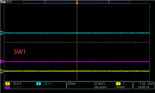
I am not sure if you understood the question in the first section (under One) but providing scope plots of the most important signals would help:
SW1, SW2, COMP
VIN, VOUT
showing a few ms and a few switching cycles.
Two: ( the second section)
1: Softstart is used to slowly ramp up the output voltage to avoid a huge inrush current into the output caps which would trigger the over current protection.
2. VOSNSN is used internally (together with VISNS) to define the operation mode
3. PGOOD is just a status signals which indicates the output voltage is settled - see also Datasheet for more details - it works as open drain, so needs a pull up.
Hello, may I ask what role do these two pins VISNS and VOSNS play for the chip? In your previous answer you said define operating mode what mode are you referring to? What happens to the chip if I leave these two pins hanging? Thank you very much for your guidance
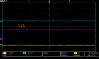
There is another question I would like to ask you about the vcc regulator inside the chip. After we power on, the output vcc voltage will have a maximum of 12v and a minimum of 3v clutter, and the clutter will increase with the increase of load. May I ask what is going on?
If necessary, we can provide you with our pcb file, but we want to send it to you privately, how should we send it to you? Thank you very much for your guidance
Hello, about this MODE pin If I choose to enable ccm mode, what impact will this mode have on lm5176? What MODE does the lm5176 work in if I turn off ccm mode with the mode pin? What will happen to lm5176? What should the MODE pin signal look like? Is it the voltage within the voltage range as mentioned in the data? Will there be other waveforms? What about rectangular waves like triangular waves? Is it just a flat voltage?
As for the understanding of cycle-by-cycle current limit, does it mean that when the current provided to the load is too large, lm5176 will stop providing current to the load and then provide current to the load at intervals
As for the understanding of hiccup mode, does it mean that lm5176 will close the chip through hiccup mode and then open the chip at intervals when the overload current is limited to 128 consecutive cycles?
About pcb 1: Do you have any suggestions, such as how the line of each pin is going, what is the problem, and the layout 2: Our board will be switched to a 4-layer board later, do you have a look at the improvement 3: Our board was very hot under the load of 30-40w in the previous test, and the temperature of the inductor could reach nearly 100 degrees. Could you please give us some suggestions on the 4-layer board to be improved later Thank you very much for your guidance
The MODE signal is a fixed voltage - defined by the resistor connected to that pin
Cycle by cycle limit:
If the current limit is detected the actual switching cycle is stopped and the device will wait for the next cycle.
Hiccup mode:
If the current limit is detected there and Hiccup is triggered the device will stop the cycle, wait some time (hiccup time) and then start with a softstart.
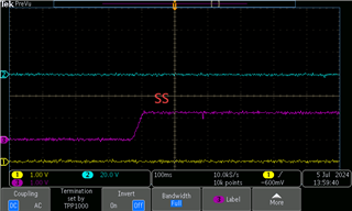
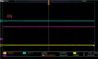
Ok, I will provide you with these signals,The input voltage I measured was 9v and the preset output voltage was 20v, all of which are based on the signals in the purple channel. Among them, the signal of ss pin I measured is when power-on, and it has been maintained at about 1.2v after power-on
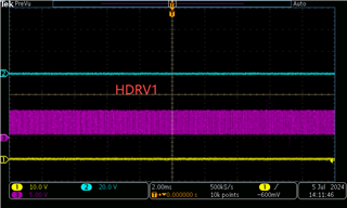
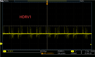
As you expected, I checked that the HDRV1 pin was disconnected from the mos, but after I reconnected, the vcc was short-circuited to the ground, which was really painful
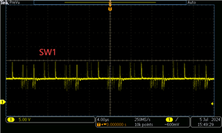
Hello, I tried to find another non-working board in which the hdrv1 and sw1 pin signals, I found two problems first: the hdrv1 pin signal is not correct, 2: the boot1 pin does not seem to work, it does not pull up the voltage of the hdrv1 pin
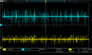
Hello, we found that the board layer has a great influence on the vcc voltage. When we use 4-layer board, the vcc voltage has almost no large ripple, while when we use 2-layer board, the highest ripple of vcc voltage can even reach 14v-15v. The following blue is the ripple of vcc. Is it caused by other reasons? (We used the layout of the LM5176EVM-HP board, and we redrew the two-layer board and four-layer board by ourselves. The following is our revised pcb file.)
the layout can have huge impact due to parasitic and generate a ringing on the switch nodes and gate driver lines. This ringing with the resulting over and/or undershoots can easily destroy some components.
If you see the large change in the VCC voltage I am pretty sure that there is a large ringing on the PCB but somehow surprised as it could not be seen in the previous measurement.
Ok, then may I ask your choice of soft start time in the case of frequent fluctuation of the input voltage is relatively large, what is the recommended soft start time
I: is the the current available for charging the output cap - this depends on the load during the startup phase (is this already loading the supply on only be enabled after the supply has started / additionally you can consider how much margin you have till you hit overcurrent limit
Thank you very much for your answer. I also want to ask what role does this comp pin play in lm5176? After I have reviewed a lot of materials, I would like to share my understanding with you to see if it is correct. comp plays a role in keeping output voltage stable, and the capacitor resistance connected with comp makes comp more stable output voltage. This is my understanding of the comp pin. If my understanding of the role of the comp pin is correct, then the resistance capacitor outside the comp pin cannot be matched at will.