This thread has been locked.

If you have a related question, please click the "Ask a related question" button in the top right corner. The newly created question will be automatically linked to this question.

ADC32RF45: Changing Sampling Rate

Part Number: ADC32RF45
Other Parts Discussed in Thread: TSW40RF80EVM, LMX2582, LMK04828

Hi,

I'm interested in changing the sampling frequency of the ADC (ADC32RF45) for my evaluation module setup (TSW40RF80EVM with TSW14J56EVM).

The examples in the User's Guide for the ADC32RF45 all have sampling frequency of 2.94912 GHz, so I was wondering if there's a guide or simple tutorial on how to change the sampling frequency?

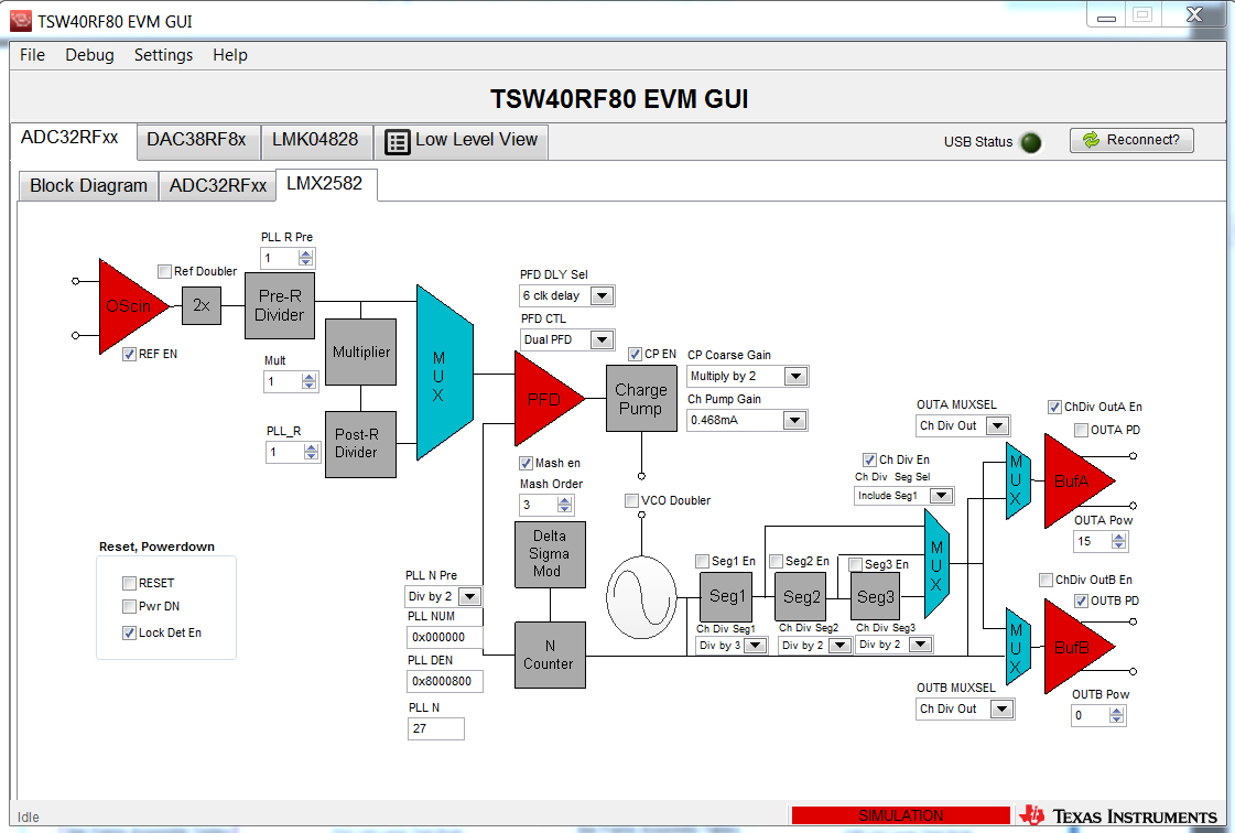
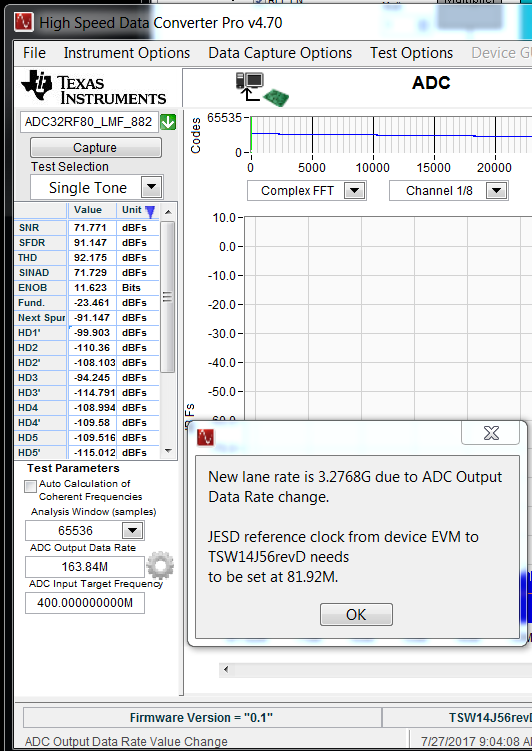
I'm currently using the TSW40RF80EVM GUI to write the ADC registers and HSDC Pro to capture the data. 

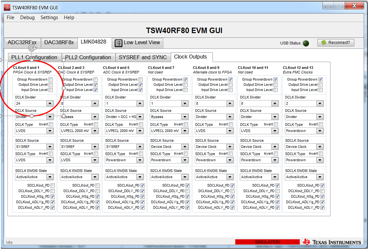
I'm using the default 122.88 MHz crystal on board as the source, and my understanding is that the LMX2582 generates the clock for the ADC.

Whenever I try to reduce the LMX2582 output frequency (by using the divide function or reduce the PLL divide-by-N), the TSW14J56EVM LED D4 stops flashing and I can no longer capture the data. Are there more settings I'm supposed to change for the ADC, or is it the TSW14J56EVM that needs to be set up differently?

Thanks

  • Hi,

    The simplest way of using an arbitrary sample frequency into the ADC32RF45 on the EVM is to use the external clocking option, where some external clock source such as a signal generator is used to bring the sample clock into the EVM.  In this case, the external clock is brought into the SMA J5 for the clock to the ADC, and a copy of that same clock signal brought into the SMA J7 for the clock into the LMK04828 clock chip.  In this case, the frequency of the sample clock can be anything that is within the bounds accepted by the ADC.   It does not have to be related to the 122.88M VCXO.   The LMK takes the external clock in lieu of any frequency that the LMK would be able to generate, and uses this external clock to generate the SYSREF to the ADC and the clock/SYSREF pair to go to the FPGA through the FMC connector.   The external clock to the ADC and to the LMK must be identical in frequency or else the SYSREF will be the wrong frequency and the whole link will fall apart.   The LMK04828 must always be part of the system because the ADC *must* have a SYSREF, and the FPGA must have a clock/SYSREF pair.  We can skip using the LMX but we cannot skip using the LMK.

    That is the external clock option.  For 'internal' clock options, there are numerous options but only one option is the default option based on how components are soldered into the EVM.  The other options would require some soldering to accomplish.

    The default internal clock option is to use the LMX2582 to generate the clock to the ADC and the LMK04828 to generate the SYSREF to the ADC and the clock/SYSREF to the FPGA.  In order for this mode to work the desired clock must be an integer multiple of the 122.88M VCXO.   That is because the LMK is being used to use one of its internal VCOs to generate a clock from the 122.88M and then make SYSREF from that.   In parallel the LMK is being programmed to generate the clock to the ADC and this also must be the same integer multiple of the 122.88M VCXO so that the SYSREF from the LMK and the clock from the LMX are 'in sync'.   The LMX has great latitude to generate other possible frequencies, but once you do the output of the LMX is no longer in step with the SYSREF from the LMK.  That is why you lose your JESD204b link.

    Another possible clock option is to resolder the AC coupling caps such that the internally generated clock to the ADC is from the LMK04828 output driver - but this mode of operation doesn't get you where you want to go.  The LMX would be out of the picture and your sample rate would still be limited by what the LMK can generate from the VCXO.

    But there *is* a mode of operation that will accomplish what I think you want to do.  It requires a bit of soldering.   The LMX2582 has *two* output drivers.   If you put the EVM in the default internal clocking mode, then one of the LMX output drivers is driving the clock to the ADC.   The other LMX output can be routed to the LMK04828 by installing the 0 ohm resistor R191 and removing the 0 ohm resistor R57.    Then the LMK04828 would be programmed just like the External clocking option that I first described because the LMK is getting its 'external' clock from the LMK.      Then the LMX can be programmed to generate any clock frequency you desire, and this frequency goes to the ADC and it also goes to the LMK so that the proper SYSREF to the ADC can be generated as well as the clock/SYSREF to the FPGA.    The LMK would get the config file used for the 'External' clocking option, but the jumper on the EVM would be set for internal clocking and the LMX would need to be programmed for the desired frequency.    The LMX would be using the 122.88M reference as the basis for this frequency generation but the LMK would not be using it - the LMK would get its clock from the LMX.  And the VCXO would not be able to be locked to an external 10M reference anymore because the input to the LMK that would otherwise have been used for the 10M reference would be taken up by the 'external' clock from the LMX.  so there wouldn't be any way to make the analog input tone to the ADC be coherent to the clocking generated on the EVM.  You would have to use a Blackman Harris windowing function on any signal data from the ADC that you wanted to do an FFT on.

    Regards,

    Richard P.

  • Hi Richard,

    Thanks for the detailed reply. For 'internal/default' clock options, I'm still having trouble keeping the JESD204B link once I change the LMX frequency to some multiples of 122.88 MHz.

    Say if I want to have a sampling rate of 1966.08 MHz (122.88 x 16) for the ADC, what else should I change for everything to work properly?

    1. SYSREF

     For the LMK04828, the default SYSREF Divider setting is 1440, so the SYSREF must be 2949.12 MHz / 1440 = 2.048 MHz

    However, when I was going through the app note SBAA221, it suggested the following equation:

    With these settings: LMFS = 8821, Decimation (D) = 12, K = 16

    SYSREF = fs / LCM(64, D*K*S) / N = 2949.12 MHz / LCM(64, 12*16*1) / N = 15.36 MHz

    But 15.36 is 7.5x 2.048 MHz. Shouldn't the divider generate a SYSREF so that 15.36 is an integer multiple of that SYSREF?

    If I'd like to operate at fs = 1966.08 MHz, then 

    SYSREF = fs / LCM(64, D*K*S) / N = 1966.08 MHz / LCM(64, 12*16*1) / N = 10.24/N MHz

    And since the LMK04828 output is at 2949.12 MHz, then I could use SYSREF Divider of 1152 to get 2.56 MHz, which is 10.24/4

    Is there a button/setting that I'm supposed to change after entering 1152 in the SYSREF Divider?

    2. JESD reference clock and FPGA Clock

    After entering the appropriate values in the HSDC Pro (1966.08 MHz Sampling Rate, Decimation 12), I get the following pop-up on recommending the clock to be 81.92MHz. 

    Is this the desired clock frequency going to the FPGA, or another CLK that I should adjust?

    I'm not sure if that's something I adjust in the LMK tab, the DAC tab, or the ADC tab

    I believe the current setting is at divide-by-24, so the FPGA clock would be 2949.12 MHz / 24 = 122.88 MHz.

    Is there a upper/lower limit at which the FPGA can be clocked at? I can't seem to find any information on that.

    Thanks,

    James

  • Hi,

    The LMK04828 cannot generate a clock of 1966.08 MHz.  The LMK04828 has an internal VCO of about 3GHz and an internal VCO of about 2.5GHz.  The LMK can only generate one of these frequencies, or a frequency that can be divided down from there such as 1.5GHz from the 3GHz.  There is no way to get 2GHz from the LMK.   The LMX can  generate that 1966.08MHz just fine.  Are you trying to run the LMX at 16x122.88 to get the 19966.08M to the ADC, but run the LMK at 24x122.88 to get 2949.12M and then 'fudge' all the dividers in the LMK by 50% higher than they would be for a straight 1966.08M clock rate?  That probably should work.  But for your decimation setting and a reference clock to the FPGA of 81.92M the divider would be a divider of 24 from the 1966.08 - but the LMK is not at 1966.08.  it would be at 2949.12 and you would need a divider of 36 to get down to 81.92M.  But the largest divider value you can get in the LMK is 32.  So you would be stuck again.  (There is a way around that.   The ini file for HSDCPro that you are using for the LMF_8821 has a line entry in there that tells the FPGA to expect a reference clock that is 1/40 that of the serial line rate.   This ini file can be edited to expect a reference clock that is 1/20 the line rate and then the LMK would be able to generate that with a divider value of 18.)     The column in the GUI for CLKOUT0 and 1 for FPGA Clock and SYSREF is where this is set.

    If we were trying to do this and the LMK were still running at the 2949.12M rate while the LMK were at 1966.08M, then besides the clock divider for the FPGA refrence clock the SYSREF divider value would have to be fudged up as well.   I do not know where you came up with a default sysref divider of 1440.  default for the LMK at power-up or reset?  one of the config files with the SPI GUI?  I do not support the TSW40RF80 EVM.  I support the ADC that is on there and I support the ADC32RF45 EVM, but it is a different group that made the TSW40RF80 and the SPI GUI for it.  I will have to bring them in to this discussion.   My suggestion earlier for using the 1966.08M from the LMX into the LMK was based on my ADC32RF45 EVM as there is an option to bring one of the LMX outputs into the LMK as an 'external' clock source.  I don't know if the TSW40RF80 supports that mode.   All of my config files use a K value of 16, and depending on the frame size for the mode chosen the SYSREF dividers I use is always one of 640, or 768, or 1028.

    SYSREF in the most basic case must simply be set to the multiframe clock rate or an integer divider value of that.  Once you pick a mode of operation then the LMFS chosen will set the size of your frame, and the K value of kframes will set the size of your multiframe.   The SYSREF must always have its rising edge on the boundary of a multiframe.  But SYSREF doesn't have to have its rising edge on every multiframe, which is why the SYSREF can be divided down by further integer values.    But the ADC32RF45 uses the SYSREF to reset other stuff as well, and so the ADC adds some additional constraints on what is an acceptable SYSREF.  That is what the equations in the datasheet are trying to portray in as simple an equation as the designers could try to express.  I may have to defer to that same group that supports the TSW40RF80.

    Regards,

    Richard P.

  • Thanks for the quick reply.

    Regarding generating the 1966.08MHz, yes I'm using the LMX for the reason you described. And I did run into the problem of not being able to divide by 36, so to get around that I used decimation of 8 (instead of 12), so that the JESD reference clock remains at 122.88 MHz. I will try editing the ini file with the method that you mentioned.

    As for the "default" SYSREF, I apologize for the confusion. I meant the default cfg file that is provided in the TSW40RF80EVM GUI, "2T2R_RevC_ConstInput_12xDec_18xInt_2949p12M_4915p2Gb.cfg". I was just curious why it was 1440 given that they had LMFS = 8821, Fs = 2949.12 MHz, and Decimation = 12. 

    So to clarify, in order for the JESD204B link to work properly, I need to

    1. use SYSREF calculated using the equation from above (SYSREF = Fs/LCM(64,D*K*S)/N)

    2. Have the proper FPGA Reference clock (122.88M if I'm using fs = 2949.12M, D = 12;  and 81.92M for fs = 1966.08M, D = 8). This reference clock is just the clock that LMK04828 supplies to the FPGA, correct? (circled in red below). Is there a lower/upper frequency limit for which the TSW14J56EVM can process?

  • E2E_1966_08_ADC_8821.cfgHi James,

    Reconfiguring the sampling clock of the ADC on the TSW40RF80EVM is not easily done through the GUI. The easiest process to change to a different sampling clock is to modify an existing configuration file, like the default one, to bring up the ADC with the sampling clock that you want.

    I have included a configuration file that configures only the ADC to run at 1966.08MHz with the following settings: LMFS = 8821 and decimation = 12. The configuration file uses the LMX to generate the 1966.08MHz clock, which will then feed into the LMK. The LMK will take in the 1966.08MHz and use it to generate the SYSREFas well as distribute the clock to the ADC and the FPGA. All you would need to do manually is to set the NCO of the ADC to whatever frequency you want.

    Regards,

    -Oscar