

In my previous post, I discussed the proper way to layout a printed circuit board (PCB) for an operational amplifier (op amp) and provided a list of good layout practices to follow. In this post, I will discuss common mistakes when laying out a PCB for an instrumentation amplifier (INA) and then show an example of a proper layout for an INA.
INAs are used in applications that require the amplification of a differential voltage, such as when measuring the voltage across a shunt resistor in a high-side current-sensing application. Figure 1 shows the schematic of a typical single-supply high-side current-sensing circuit.
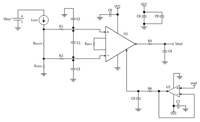
Figure 1: High-side current-sensing schematic
In Figure 1, a differential voltage is measured across RSHUNT, with R1, R2, C1, C2, and C3 providing input common-mode and differential-mode filtering. R3 and C4 provide output filtering for the INA, U1. U2 buffers the reference pin of the INA. R4 and C5 form a low pass filter that minimizes noise that the op amp introduces to the reference pin of the INA.
While the layout for the schematic in Figure 1 seems straightforward, it is easy to make mistakes in the PCB layout that might degrade circuit performance. Figure 2 shows a PCB layout with three mistakes we at TI commonly see when reviewing INA layouts.
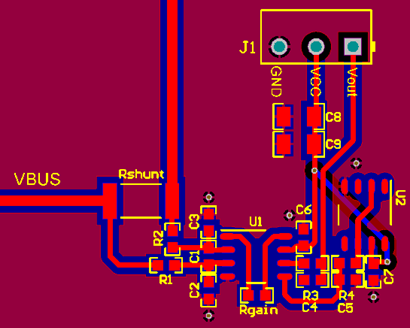
Figure 2: Common PCB layout for an INA
The first mistake is how the differential voltage is measured across the resistor, Rshunt. Notice that the trace from Rshunt to R2 is much shorter, and therefore has less resistance than the trace from Rshunt to R1. This difference in trace impedance may create a differential voltage at the input of U1 due to the input bias current of the INA. Since an INA’s job is to amplify a differential voltage, having unbalanced traces at the input can cause an error. Therefore, keep the input traces of an INA as balanced and as short as possible.
The second mistake is related to the gain-setting resistor of the INA, Rgain. The traces from the pins of U1 to the pads of Rgain are longer than necessary, which create additional resistance and capacitance. Having additional resistance may introduce error in the desired gain of the INA, since the gain depends on the resistance between the INA’s gain-setting pins, pins 1 and 8. Additional capacitance may cause stability issues because the gain-setting pins of the INA connect to the feedback node inside the INA. Therefore, keep the traces connected to the gain-setting resistor as short as possible.
Finally, the positioning of the reference pin buffer circuit may need improving. The reference pin buffer circuit is positioned far from the reference pin, which increases the resistance connected to the reference pin and opens up the possibility for noise and other signals to couple onto the trace. Additional resistance on the reference pin will degrade the high common-mode rejection ratio (CMRR) that most INAs provide. Therefore, position the reference pin buffer circuit as close to the reference pin of the INA as possible.
Figure 3 shows a layout that corrects these three mistakes.
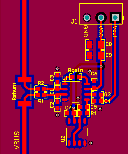
In Figure 3, you can see that the traces from the shunt resistor to R1 and R2 are equal lengths and have a kelvin connection. The traces from the gain-setting resistor to the pins of the INA are as short as possible, and the reference buffer circuit is as close to the reference pin as possible.
The next time you lay out a PCB for an INA, be sure to follow these guidelines:
- Keep all traces on the input perfectly balanced.
- Reduce trace length and minimize capacitance on the gain-setting pins.
- Position the reference buffer circuit as close to the reference pin of the INA.
- Place decoupling capacitors as close to the supply pins as possible.
- Pour at least one solid ground plane.
- Do not sacrifice good layout to label a component with silkscreen.
- Follow the guidelines in my previous post.
Additional resources
- Find commonly used analog design formulas in the Analog Engineer’s Pocket Reference by Art Kay and Tim Green.
- Check out the TI Designs 10µA-100mA, 0.05% Error, High-Side Current Sensing Solution Reference Design (TIPD135).
- Explore TI’s entire portfolio of amplifier ICs and find technical resources to help with your design.
- Review all of TI’s available precision Instrumentation Amplifiers
- Use TI’s Universal Instrumentation Amplifier Evaluation Module to test your instrumentation amp sample
- Read up on tips and tricks for getting the most out of your instrumentation amplifier design
