

This technical article was updated on July 23, 2020.
My previous post discussed the requirements for a high-throughput data-acquisition (DAQ) system and how to select the right precision op amp to drive the SAR ADC. In this post, I’ll discuss the circuit configuration required to drive the SAR ADC, how that circuit configuration affects operational amplifier (op amp) stability, and the measured data of the OPA625 op amp settling to 16 bits in less than 500ns in a design with the ADS8860 ADC.
Step 1: Size the capacitor in the RC charge bucket
Figure 1 shows the circuit configuration required to drive the ADS8860 with the OPA625. The charge-bucket portion of the circuit consists of the capacitor, CFLT, and resistors, RFLT. The charge bucket has two main functions. The first is to reduce kickback noise caused by the internal switching in the ADS8860. The second is to quickly charge the sample-and-hold capacitor of the ADS8860. The gain network consists of RF, RI and CF. The gain network sets the DC gain and helps stabilize the OPA625.

Figure 1: ADS8860 driving circuitry
Equation 1 shows how to calculate the value for CFLT:
 (1)
(1)
The sample-and-hold capacitor of the ADS8860 is 59pF; therefore CFLT must be at least 1180pF. Choosing the closest standard value of capacitors, let’s use 1200pF.
Step 2: Balance the capacitor with a resistor
Having a capacitive load on the output of an op amp degrades a device’s phase margin. Therefore, we must use a resistor, RFLT, to help stabilize the OPA625. Although a large RFLT resistor value will increase the phase margin substantially, it will also increase the settling time. To balance phase margin and settling time, RFLT was selected to be 12Ω.
This application requires a DC gain of 2V/V. Equation 2 shows the gain equation for a noninverting op amp.
 (2)
(2)
Setting RF = RI = 5kΩ yields a gain of 2V/V.
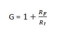
Figure 2 shows the phase margin of the OPA625 based on an RFLT of 12Ω, gain-setting resistors of 5kΩ and no CF.
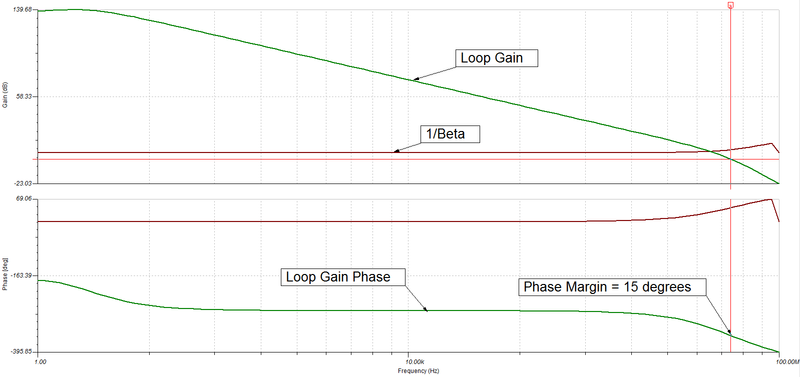
Figure 2: Phase margin with no CF
Without a feedback capacitor, the OPA625 only has 15 degrees of phase margin. For the OPA625 to be considered stable, I need at least 45 degrees of phase margin. Figure 3 shows the phase margin of the OPA625 using a 1pF capacitor for CF.
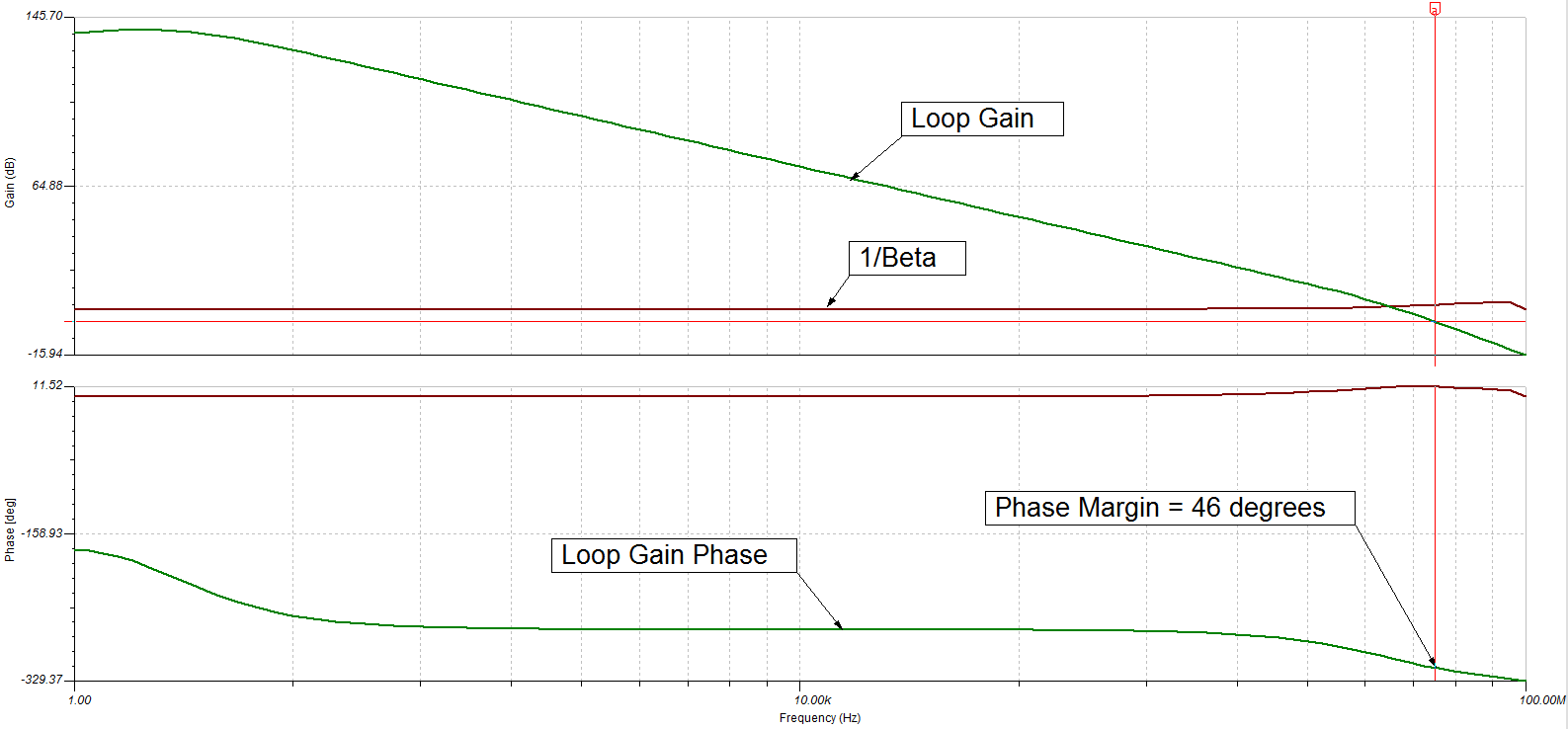
Figure 3: Phase margin with CF=1pF
The results
Using a 1pF capacitor for CF increases the phase margin to 46 degrees, so the OPA625 is now considered stable.
Figure 4 shows the final circuit configuration and component values.
Figure 4: Final circuit configuration
Figures 5 and 6 show measured data of the OPA625 driving the ADS8860 and settling to one-half least significant bit (LSB) in 360ns.
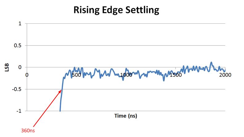
Figure 5: Rising edge settling
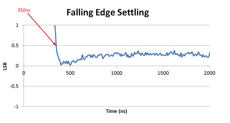
Figure 6: Falling edge settling
By choosing the OPA625 as the ADC driver, sizing an appropriate capacitor for the charge bucket, and balancing RFLT and CF to stabilize the OPA625, I was able to obtain my design goal of settling to one-half LSB in less than 500ns. So the next time you need to achieve fast settling for a high-performance multiplexed DAQ system with high throughputs, consider using the OPA625.
Additional resources
- Download data sheets for the ADS8860 and OPA625.
- Watch on-demand training courses on stability and more in TI Precision Labs – Op Amps.