As a good, cynical and sarcastic analog engineer I am negative at times about a lot of things. However, from experience, I am here to tell you to never be negative about single supply comparators, especially if you want things to happen in a timely manner!
The TLV3701 is a “nanopower comparator” which uses a low quiescent power supply current of 560nA, typical. From the key specifications listed in Figure 1 we see the propagation delay time from high to low, t(PHL), is specified at 37us for 50mV of differential input overdrive.
Figure 1
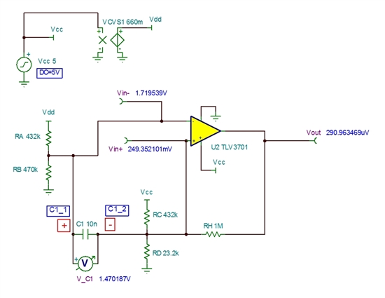
A customer of mine, who happens to be a Digital Design Engineer dabbling in analog, sent in the nanopower comparator circuit in Figure 2. Now old “One Bit” (real name withheld to protect the guilty) was propagating on about how Texas Instruments parts never meet the datasheet and in particular how the propagation delay specification was off by a factor of x62 too long, between the datasheet and his real application. Shown in Figure 2 are the DC values of old One Bit’s single supply comparator circuit. Note that there was a concern of noise causing false triggering of the comparator, so capacitor C1 was added between the Vin+ and Vin- of the comparator.
Figure 2
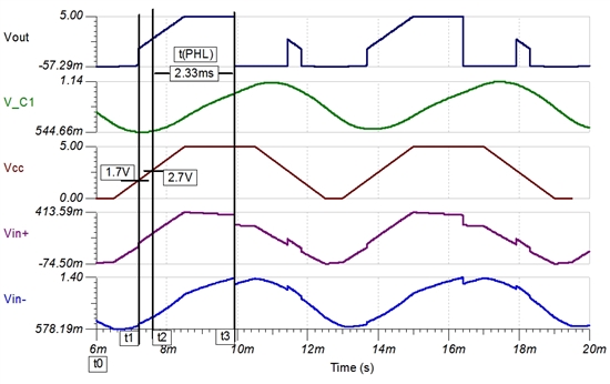
Figure 3 shows the waveforms for operation of the comparator circuit. During power cycling of Vcc, the propagation delay from high to low was observed to be 2.33ms (data sheet specification is 37us). The propagation delay is measured from the time Vcc reaches the minimum supply voltage of the part (2.7V) until Vout goes to its proper state based on the voltages at Vin+ and Vin-. During this entire power cycle Vin- is greater than Vin+ and so Vout should be at 0V. Note that the respective resistor dividers for the Vin+ and Vin- result in a differential voltage across capacitor C1. The result is that Vin+ of the comparator is at a lower voltage than the Vin-. At a first order glance, when the Vcc goes to zero, it will take a while for the voltage across the capacitor to discharge to zero, because of the large values of resistors used in the Vin+ and Vin- voltage dividers.
When Vcc is at zero volts (Time=t0) Vin+ of the comparator is at -74.5mV and since there is a 1meg-ohm resistor, RH, from the comparator output to Vin+ the output, Vout, is also left at a -57.29mV. At Time=t1, where Vcc=1.7V, the comparator internal circuitry begins to come alive, but the output follows the supply as there is not adequate voltage to properly bias all internal circuits correctly. This is a common observation for many op amps and comparators on power-up, until the minimum specified supply voltage is reached. At Time=T2, Vcc has reached the minimum supply of 2.7V for the comparator and propagation delay is measured from T2 until T3 where Vout goes to its proper 0V state.
So why is the time between T2 and T3 not the datasheet specification of 37us? Remember the TLV3701 quiescent supply current is only 560nA, typical. That is not much current to charge up all internal capacitances inside to reach the proper state when Vcc=2.7V minimum. This is especially true when the voltages across these internal capacitors do not start at 0V but rather at negative voltages! So how do we stop all of this negativity about single supply comparators and still maintain our noise filtering on Vin+ and Vin-?
Figure 3
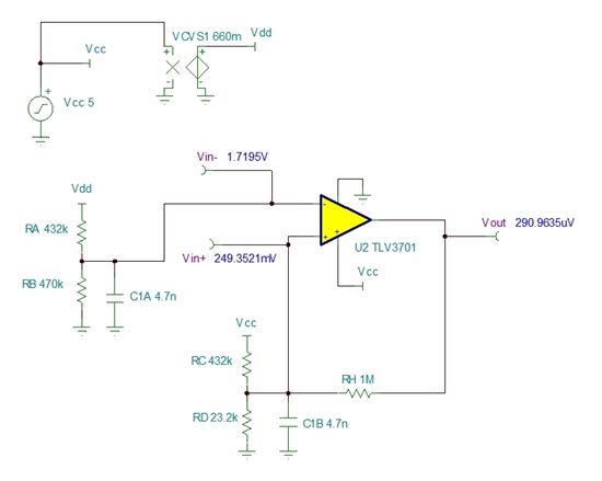
In Figure 4 we revise old One Bit’s circuit to leave noise filtering but remove the negativity associated with his circuit. By splitting C1 into C1A and C1B, as shown, we can filter each of Vin+ and Vin- to GROUND for effective noise filtering without creating any negative voltages during power cycling on Vcc.
Figure 4
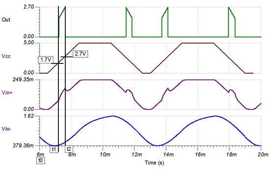
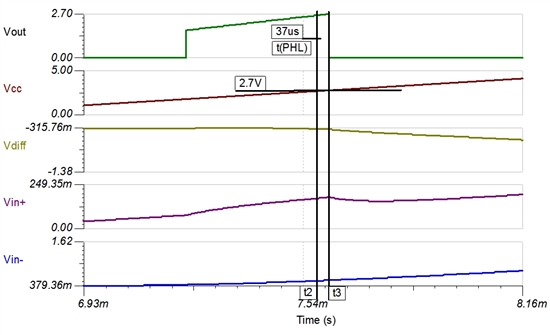
We subject our modified comparator circuit to the same Vcc cycling as One Bit’s original circuit as shown in Figure 5. Note the propagation delay cannot be seen around t2, since it has become so short. In Figure 6 we zoom in around t2 to see the propagation delay between t2 and t3 measured to be the datasheet specification of 37us.
Figure 5
Figure 6
So the moral of the story here is negative attitudes can produce unwanted project delays and negative voltages on single supply comparators will introduce unwanted propagation delays! Fortunately, the analog engineering solution is a simple bypass capacitor from each of Vin+ and Vin- to GROUND.
Sign up to get our blog pushed to your inbox, scroll to the top and look for this -->


