

Package level trim is a semiconductor manufacturing method that achieves highly accurate amplifiers and other linear circuits. The key measurement of accuracy for an amplifier is its input offset voltage. The input offset voltage is an error voltage at the input of the amplifier measured in microvolts. This error voltage can range from tens of microvolts to thousands of microvolts.
Amplifiers and other semiconductor devices are built through a chemical process called fabrication. During fabrication thousands of amplifiers are grown on a silicon disk called a wafer. Each amplifier is composed of thousands of transistors, resistors, and capacitors. The input offset error is caused by mismatch of the input transistors on each amplifier. Ideally each transistor is identical, but in practice the semiconductor manufacturing process is not perfect so there is variation from transistor to transistor.
After the wafer is fabricated it is tested in the wafer form. During the wafer test, some amplifiers use a process called laser trim where the offset of the device is adjusted with a laser by measuring and physically cutting the microscopic resistors on each device. This process is time consuming and expensive. Furthermore, some of the accuracy improvement gained in wafer form is lost when the device is removed from the wafer and packaged in the standard plastic package (See Figure 1). This is because the packaging process introduces stress on semiconductor die causing the offset error to shift. Despite the shortcomings, the laser trim method is still widely used and does provide significant accuracy improvements.
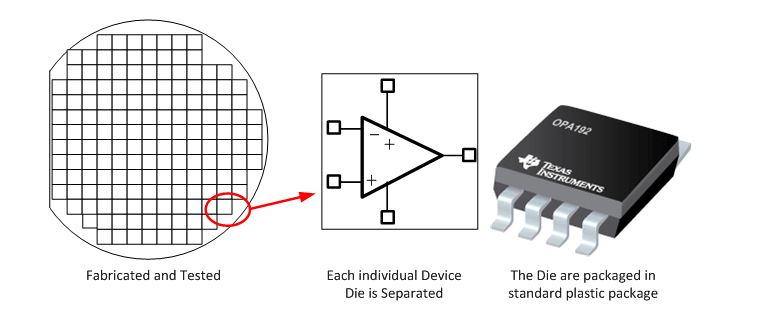
Figure 1: Manufacturing process for semiconductor devices
Auto-zero correction is another method to minimize the offset error. In this case, an error correction circuit is included with each amplifier that measures the offset and adds a signal to counteract the offset error. This circuit requires digital control and adds cost and complexity to the design. More importantly, some noise and signal aliasing effects are caused by the periodic nature of the digital circuit. Despite these shortcomings the auto-zero correction and other digital correction methods are effective and commonly used techniques for minimizing offset error.
A third way that offset is reduced is package level trimming of the device. This method is similar to wafer trim in that resistors are adjusted on the input stage to correct the offset voltage. However, in this case, the adjustment is done after the devices are in their final package. This is typically done by applying a digital signal to the output during the final package level manufacturing test. After the trim is complete, the trim control circuit is disabled and the adjustment becomes permanent. Package level trim is often called e-TrimTM, TI’s patented package-level trimming architecture, because the trim is done using digital signals rather than laser trimming or other traditional methods. See Figure 2 for an illustration of the package level trim method.
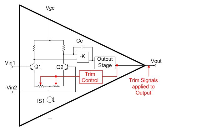
Figure 2: Package level trim method
Package level trim has some advantages over the other offset adjustment methods. Remember that in the case of laser trimming the adjustment is done before the packaging and some of the offset correction is lost by stresses introduced in the packaging process. In the case of package level trimming, the adjustment is done after the packaging, so this method is not affected by packaging stresses. The end result is that this method produces lower, more accurate, offset voltages. Also, this method is faster than laser trimming which reduces costs.
There are also some advantages of package level trimming over auto-zero correction. Remember that in the case of auto-zero correction, the digital correction circuit introduces some noise and aliasing effects. The package level trimmed device does not have these issues because the adjustment of the internal trim resistors is only done once during the manufacturing of the device whereas the auto-zero correction is done continuously during the device’s operation.
In general, the package level trim method is a very effective technique for increasing the accuracy of analog circuits. This method has some advantages over traditional methods. The OPA192 is an example of a new device that uses the package level trim method to achieve very good offset accuracy.

