Figure 1
The diagram in Figure 1 is a 3-wire analog output module that uses a dual-channel DAC8562 digital-to-analog converter (DAC) to drive voltage and current output stages with the high-voltage, 36-V OPA192 operational amplifier (op amp).
The current output is a two-stage, high-side, voltage-to-current converter. The second stage – made up of amplifier A2, MOSFET Q2 and sense resistor RB – delivers the output current to the load. A2 regulates the output current through negative feedback by sensing the voltage drop across RB at the inverting input node. This ensures it is equal to the voltage applied to the non-inverting input.
If you used this stage alone, noise or other switching transients on the high-side supply would directly contribute noise to the output. This is because the voltage at the non-inverting input of A2 will not move ratiometrically with the high-side voltage.
To avoid this issue, add the first stage to the design to create a current mirror that enhances the system’s immunity to noise on the high-side supply. The first stage uses amplifier A1, MOSFET Q1 and resistor RSET to create a current sink.
In this block, A1 uses negative feedback to drive the gate of Q1. This regulates the current flow through Q1 such that the voltage developed at the high-side of RSET is equal to the voltage at the non-inverting input of A1. The current flowing through RA develops a voltage drop from the high-side supply at the non-inverting input of A2 that drives the second stage.
The ratio of resistors RA and RB gains up the current flowing through RSET in the first stage to the current output that goes to the load. Since all current flowing through the first stage goes to ground instead of the load, the gain set by RA and RB directly sets the efficiency of the system.
Check out our TI Designs verified reference design (TIPD102) for an in-depth look at how to design this voltage-to-current converter, including full theory of operation, component selection, stability criteria, modifications, PCB layout and measured results.
The voltage output stage of the design in Figure 1 is considerably easier to understand compared to the current output. Amplifier A3 in this circuit is in a modified summing amplifier configuration. RFB and RG1 apply gain to the DAC output applied to the non-inverting input. Meanwhile, RFB and RG2 use the reference voltage of the DAC to apply an offset to the output signal that can be scaled by the ratio of RFB and RG2.
With the right resistor values, this versatile circuit can scale most conventional low-voltage DAC outputs into the common industrial voltage ranges of 0-5V, 0-10V, +/-5V, and +/-10V. Check out our industrial voltage drivers reference design (TIPD125) to learn more.
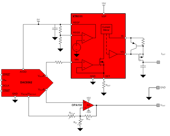
Figure 2
In the 1980s, TI introduced a family of devices with the “XTR” prefix that simplified the design of high-side current outputs by integrating most of the components required to realize the voltage-to-current converter and utilizing conventional low-voltage DAC outputs to generate a variety of current outputs. Figure 2 shows an example with the XTR111 precision voltage-to-current converter/transmitter.
Our new DAC8760 family also simplifies the design of these systems. The family integrates the voltage and current output stages, as well as the DAC and reference – all while delivering impressive accuracy and reliability.
Be sure to check out the series about transients and transient immunity standards in the industrial space from my colleague Ian Williams. In my next post in this series, I’ll explain how to design circuits to protect 3-wire analog outputs from the transients Ian discusses.
Related how-to content:
- Learn about analog outputs and architectures in my last blog post in the Industrial DACs series.
- Get more pointers about how to design with precision DACs in the DAC Essentials blog series.
- Watch a video on how to design analog outputs for industrial control applications with 4-20 mA DACs.

