Three… two…one…happy New Year!
As the fond memories of 2014 give way to the exciting possibilities of 2015, many people begin the New Year by making resolutions: some modulate their junk food intake; others filter out a bad habit; a few even integrate exercise into their daily routine. And while these are all great ideas, I propose we ring in the New Year with a different kind of resolution – delta-sigma (ΔΣ) analog-to-digital converters (ADCs)!
Happy New Year!
What do ΔΣ ADCs have to do with resolution, you ask? Everything! ΔΣ ADCs are all about the resolution – up to 32 bits in fact. By taking advantage of oversampling and noise-shaping techniques, they’re able to provide the highest resolution capabilities of any ADC architecture available today – all using a 1-bit ADC (in the simplest case).
How is it possible to get so much out of so little? To find out, read our monthly blog series in 2015 where my colleagues and I in TI’s Precision ΔΣ team will discuss all aspects of the ΔΣ ADC, from general operation to specification analysis to applications/helpful hints. For now, we’ll begin with a simple overview of ΔΣ ADCs: how they work, why we use them and where to find them.
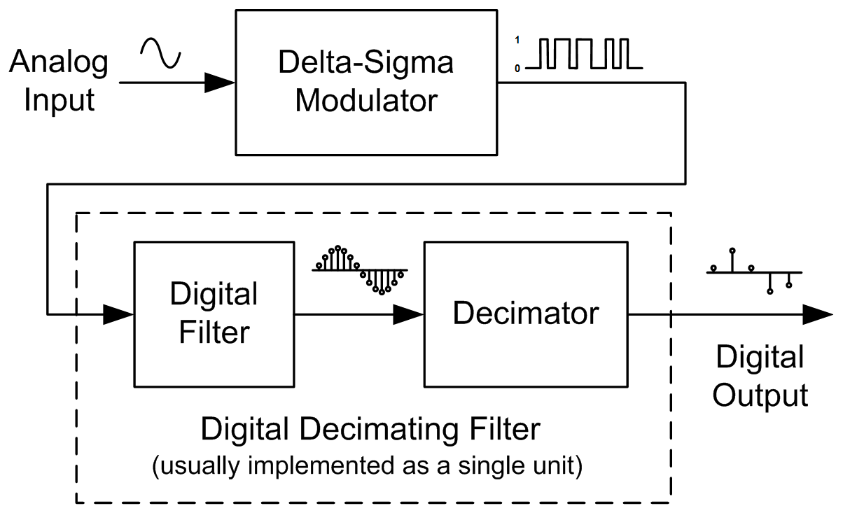
First things first: why do we call them ΔΣ ADCs? Well, this architecture consists of two core components: the ΔΣ modulator and the digital decimating filter (Figure 2). Inside the modulator, we take the difference (Δ) of the input signal and the sum (Σ) of the error voltages to generate a bitstream of 1s and 0s that represents the analog input. We then filter this bitstream to remove high-frequency noise, thereby increasing resolution, and decimate the result to achieve the desired output data rate.
For an in-depth analysis of each component, read our upcoming posts in the “Delta-sigma ADC basics” blog series.
Figure 1: The ΔΣ modulator/digital filter block diagram
However, there’s more to ΔΣ ADCs than these two core components and excellent resolution. One benefit common to many of these devices is a high level of integration, as many are targeted for certain end equipment or applications that need specific components to operate.
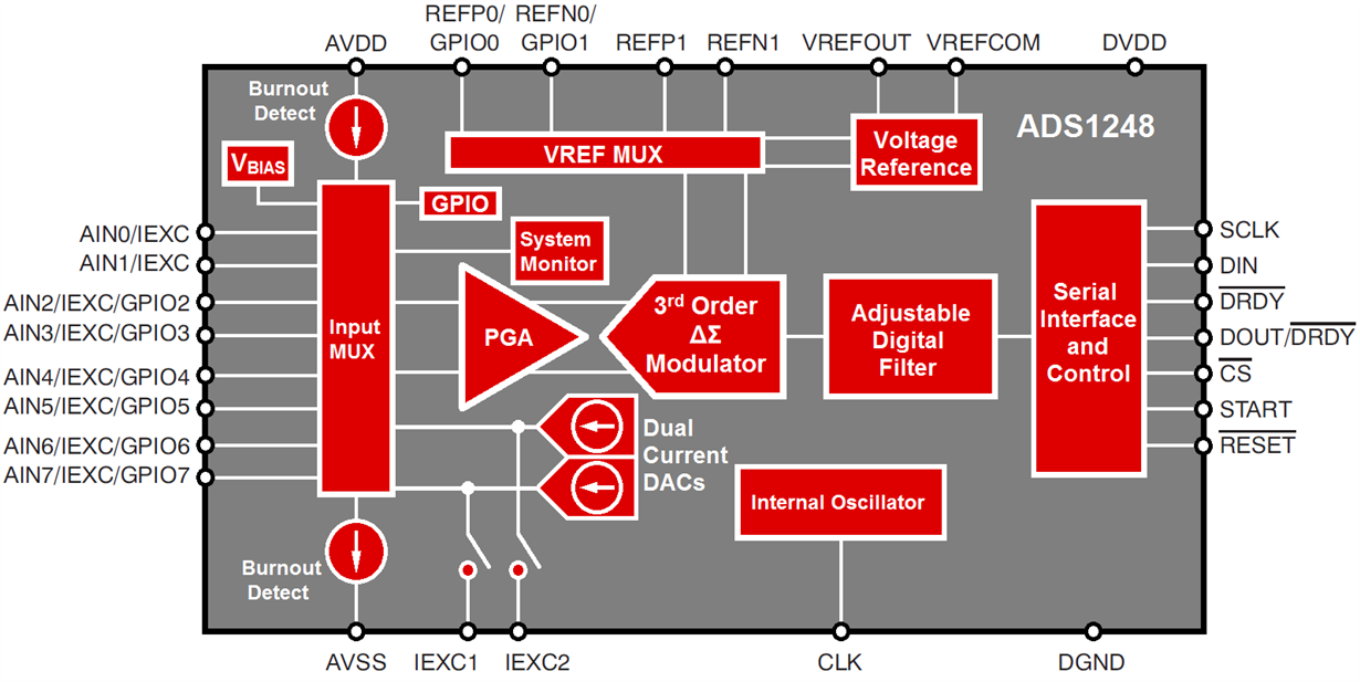
To satisfy these requirements, ΔΣ ADCs often include a number of features such as programmable gain amplifiers (PGAs), internal voltage references, oscillators, general purpose input/output (GPIO) pins, temperature sensors, burnout current sources, system monitoring/calibration, and excitation current sources. The ADS1248 functional block diagram in Figure 3 shows an example of this level of integration.
Figure 2: ADS1248 system functional block diagram
Engineers make use of the excellent resolution and high integration of ΔΣ ADCs in a wide range of applications. High resolution lends itself to the high-end weigh scale arena, while the high level of integration enables easy RTD and thermocouple measurement, demonstrated by the RTD Temperature Transmitter (Figure 3). Additionally, you’ll find ΔΣ ADCs in a host of other industrial electronics, as well as in energy-metering applications (ADS131E08) and medical equipment (ECG/EEG machines) (ADS1299). Developers even utilize these ADCs in the automotive sector (ADS1120-Q1), given the need for more fuel-efficient cars and the increasing popularity of electric vehicles.
So, now that you know how ΔΣ ADCs work, why you would use them, and where to find them, what next? Since we’ve only begun to scratch the surface of the capabilities of this ADC architecture, keep an eye out for the “Delta-Sigma ADC basics” blog series throughout the year to learn more about the details of the ΔΣ ADC, delve into its different specs, and understand several applications for getting the most out of your device.
Until then, have a happy new year, and don’t forget about those resolutions!
Additional resources:
Check back each month to read the “Delta-Sigma ADC basics” blog series.
Learn more about ADS1248 24-bit ADC.
Small Form Factor, 2-Wire 4 to 20mA Current Loop RTD Temperature Transmitter Reference Design


