Whenever I review a schematic or a PCB layout for a younger engineer, I make a point to pick out items and simply ask them “why?” Why did you choose this component? Why did you place it here on the PCB? My point in asking these questions is that every design decision should have a valid reason that the engineer understands.
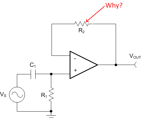
For example, a resistor in the feedback path of an op amp configured as a buffer provokes an immediate “why?”
Figure 1: An op amp buffer circuit with a resistor included in the feedback path
The ugly truth is that often an engineer doesn’t know why he or she included resistor R2. They may have seen it on a previous schematic and felt obliged to include it. Most commonly, these resistors are used in low speed applications (<50 MHz) to cancel the DC offset produced by the input bias current of the op amp. However, as my now-retired colleague Bruce Trump pointed out in an article on input bias current cancellation resistors, this is rarely effective.

Download our e-book on op amp design
| From voltage-range issues to input bias current, The Signal e-book covers a variety of op amp topics for your next design. |

R2 may also provide some protection to the inverting input in the event of an ESD strike at the output. Also, some op amps, especially JFET input types, may produce lower distortion if both inputs have matched source impedances. But without understanding the purpose of R2, the value is often selected randomly, leading to instability.
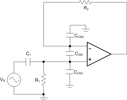
To understand how R2 causes instability, let’s add the input capacitance of the op amp to the circuit as shown in Figure 2.
Figure 2: Op amp input capacitances added to the circuit of figure 1
R2 forms a low pass filter at the inverting input with the input common-mode capacitance CCM2 and the input differential capacitance CDM. The low-pass filter in the feedback path produces a zero in the noise gain curve (1/β) of the amplifier at the frequency:
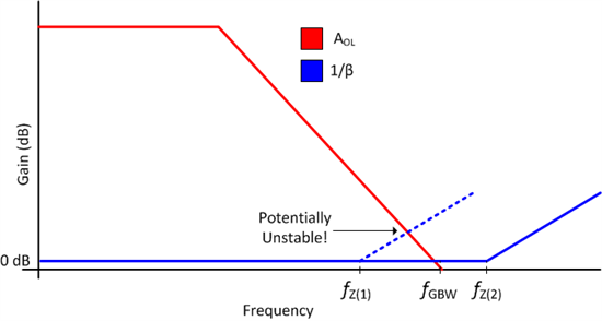
If this zero occurs far above the unity gain bandwidth of the amplifier, as shown by fz(2) in Figure 3, it should not affect the stability of the circuit. However, if the zero occurs at or below the unity gain bandwidth of the op amp, like fz(1), the noise gain curve will intersect the open loop gain curve at greater than 20dB/decade, indicating probably instability.
Figure 3: Open loop gain (red) and noise gain (blue) curves for a buffer amplifier
The phase shift from this zero will begin 1 decade below fz, so a conservative design guideline is:
By substituting the equation for fz, we can determine the maximum value for R2 to ensure stability:
To show this effect, I simulated an OPA172 in a buffer configuration and measured the phase margin for different values of R2. The unity gain bandwidth of the OPA172 is 10MHz and the input common-mode and differential capacitances are both 4pF. Using the design guideline in equation 4, the maximum value for R2 is:
The TINA-TI™ simulation schematic I used to measure phase margin is shown in figure 4. The feedback loop is broken at the op amp output by inductor L1 and a source (VG1) is AC coupled into the feedback loop. The loop gain is given by the probe labeled “LG” and phase margin is measured when the loop gain = 0dB.
Figure 4: TINA-TI™ simulation schematic for an OPA172 configured as a buffer
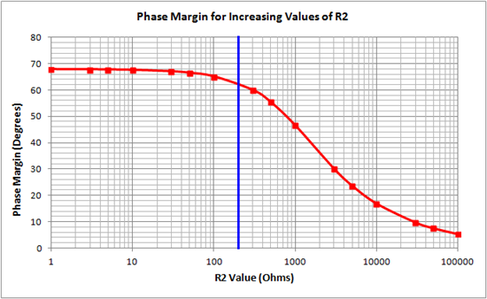
Figure 5 is a plot of the phase margin as the value of R2 is increased. The blue line is the maximum value of R2 we calculated in equation 5. Below this limit, the reduction in phase margin is minimal, with it falling to 62° at R2 = 200 Ohms. Above this limit, the phase margin decreases rapidly.
Figure 5: Plot of phase margin versus R2 value for the OPA172
Remember that this analysis doesn’t include the effects of capacitive loads or PCB parasitics, which will also degrade the phase margin of the circuit.
In some circuits there may be a valid reason to include R2, but ask yourself what you’re trying to accomplish with this resistor before putting it in the schematic. If the required value is large, you’re probably headed for stability problems. Asking yourself “why” in any engineering pursuit is crucial to improving as an engineer!


-

Soufiane Bendaoud
-
Cancel
-
Vote Up
0
Vote Down
-
-
Sign in to reply
-
More
-
Cancel
Comment-

Soufiane Bendaoud
-
Cancel
-
Vote Up
0
Vote Down
-
-
Sign in to reply
-
More
-
Cancel
Children