

Two commonly asked questions when designing an operational amplifier into a new application are:
- What is its “typical” power dissipation?
- What is its “maximum” power dissipation?
Most often these questions are asked in conjunction with other questions regarding the device’s various thermal resistance characteristics. These are part of a standard bank of questions used to gauge a device’s power-handling capability and help disclose any potential long-term reliability concerns.
An amplifier’s data sheet may not list power dissipation information, but usually it does provide the operating voltage range, and typical and maximum operating currents. Answering the first question about “typical” power is normally straightforward. It is a matter of applying the power formula, PDQ = VS∙IQ, where PDQ is the quiescent power, VS is the supply voltage and IQ is the “typical,” quiescent operating current.
Let’s use the CMOS OPA316 operational amplifier as an example and calculate its “typical” power. Its voltage range and operating current are provided in the data sheet as shown here:
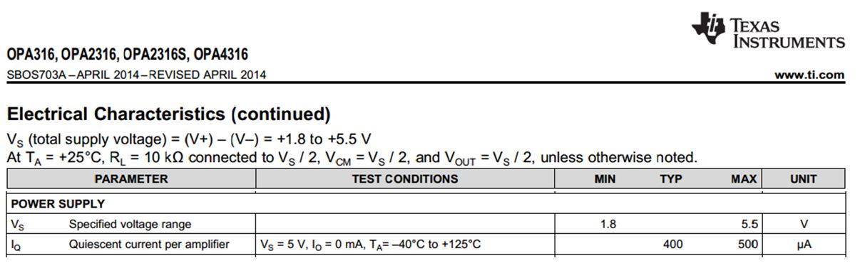
The supply range is specified as +1.8 to +5.5 V, with a typical IQ of 400 μA. Figure 1 shows a simple measurement circuit. Assuming a nominal, 5 V supply voltage and applying VS∙IQ, the “typical” power, PDQ, is 2 mW. Easy enough!

Figure 1 OPA316 configured to determine quiescent power dissipation
Maximum power is a different story because customers don’t often state the operating conditions. Quite often it is left to the applications engineer to try and surmise what the customer wants. Do they need the maximum power when the amplifier is operating in a normal linear mode, or in some extreme condition?
This will be the subject of Part 2 of this blog series. Our discussion will continue soon on maximum power dissipation, but please subscribe to ensure you don’t miss our next segment of this blog!