

Join me for the first in a three part series...
The transimpedance amplifier is a common op amp application with an output voltage that depends on the input current and a feedback resistor:

Quite often I see this circuit used to amplify the output current of a photodiode as shown in Figure 1. Almost all transimpedance amplifier circuits require a feedback capacitor (CF) in parallel with the feedback resistor to maintain stability by compensating for parasitic capacitances at the inverting node of the amplifier.
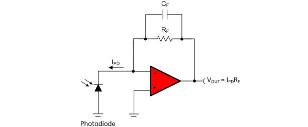
Figure 1: Feedback capacitor CF compensates for the photodiode junction capacitance and op amp input capacitance.
Numerous articles exist on how to select a feedback capacitor when using a certain op amp, but I think this is the wrong approach. Despite what we semiconductor manufacturers love to believe, engineers don’t start with an op amp and go looking for a circuit to build with it! Most engineers start with a list of performance requirements, and look for parts that will meet those requirements.
With that in mind, a better approach would be to determine the largest feedback capacitor allowable in our circuit and then select an op amp with a sufficient gain bandwidth product (GBW) to be stable with this feedback capacitor.
Here’s a simple step-by-step approach to determine the required op amp bandwidth for a transimpedance amplifier.
Step 1: Determine the maximum allowable feedback capacitance.
The feedback capacitor, in combination with the feedback resistor, forms a pole in the frequency response of the amplifier:

Above this pole frequency, the amplification of the circuit will decline. The maximum feedback capacitor value can be determined from the feedback resistor and the desired bandwidth:
 By keeping the feedback capacitor at or below the value calculated in equation 3, we ensure that our circuit will meet our bandwidth requirements.
Step 2: Determine the capacitance at the inverting input of the amplifier.
In Figure 2, the circuit in Figure 1 has been redrawn to show the junction capacitance of the photodiode (CJ) and the differential (CD) and common-mode (CCM1, CCM2) input capacitances of the amplifier. These values are typically given in the op amp and photodiode datasheets.

Figure 2: Transimpedance amplifier circuit showing capacitances at the inverting node.
From this illustration it is apparent that CJ, CD, and CCM2 are in parallel and the capacitance at the inverting input is:

CCM1 does not contribute to the input capacitance because the non-inverting terminal is grounded. CD, and CCM2 may not be known at this time since we haven’t yet selected a specific op amp. I often use 10pF as a reasonable guess for the sum of these values. The exact value can be substituted later to confirm the appropriateness of a specific op amp.
Now that we’ve determined our values for CF and CIN we’re ready to calculate the required op amp bandwidth. In the next part of this blog I will explain this calculation and use this process in a design example.
Stay tuned!