

In my previous post in this series on understanding voltage references, I talked about the ways to build a shunt reference with a precision of series voltage reference. In this blog I will discuss how to design a new precision voltage reference by level-shifting existing references.
Due to circuit topology limitations, some of the highest-precision series voltage references do not offer lower output-voltage options like 1.25V. But as long as a negative supply is available, there are ways to create it by using one of the existing references as a basic building block. The newly built voltage reference’s initial accuracy and drift can closely match the performance of the original voltage reference, as long as the input voltage offset and drift of the external operational amplifier (op amp) – as well as matching of the resistors used – meet the appropriate minimum requirements. 
One of the ways to generate a 1.25V precision voltage reference involves voltage-level translation, shown in Figure 1. The REF5025 nominal output voltage (2.5V) is level-shifted to half of its value by driving its GND pin to -1.25V with the use of the OPA376. Since the maximum input-voltage offset and drift of the OPA376 are +/-25µV and +/-1µV/C, respectively, and as long as the matching of R1/R2 resistors is within 0.01%, the resulting 1.25V voltage reference initial accuracy and drift will match the REF5025’s performance.
The resulting 1.25V reference can work on power supplies as low as +/-1.35V or as high as +/-2.75V; it can also be powered by asymmetric supplies of +1.35V/-4.15V, +4.15V/-1.35V or anything in-between, as long as the total supply voltage does not exceed the OPA376’s 5.5V maximum supply.
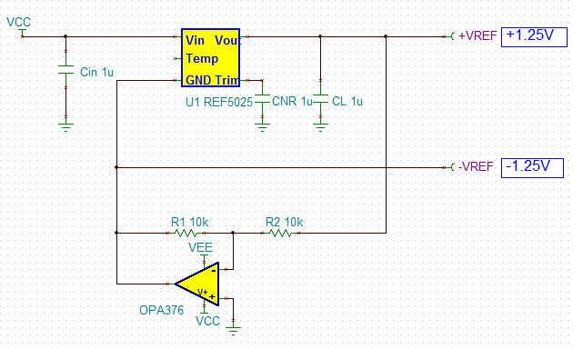
Figure 1: Creating a 1.25V precision voltage reference
In order to create a higher-output precision voltage reference, one may use the REF5010 together with the INA149 difference amplifier shown in Figure 2. Since the INA149 is a precision unity-gain difference amplifier with a maximum gain error of 0.02%, as well as maximum Vos and drift of 1100µV and 15µV/C, respectively, using it in combination with a 10V precision voltage reference results in a 0.011% input offset-related error (1100µV/10V*100%) and 1.5ppm/C temperature drift (15µV/C/10V*1E+6). These parameters are within the specified maximum initial accuracy and temperature drift of the REF5010 and thus ensure that the dual-output precision voltage reference shown in Figure 2 closely preserves the initial accuracy and drift of the REF5010 building block.
As far as power supplies go, the circuit configuration shown in Figure 2 can work on the minimum supplies of +5.2V (limited by the 200mV maximum dropout voltage of the REF5010) and -6.5V (the output of the INA149 can operate linearly down to 1.5V of its negative supply.) On the high end, the maximum positive supply can be as high as 13V (limited by the 18V maximum total supply of the REF5010), while the negative supply, Vee, is limited only by the 36V maximum total supply of the INA149, and thus can operate from 30.8V (in case Vcc = 5.2V) or 23V ( for Vcc = 13V).
It might be worth pointing out that the use of the difference or instrumentation amplifiers like the one shown in Figure 2, with superb laser-trimmed internal resistors and temperature coefficients matching, typically results in a higher-performance and lower cost solution than using the external resistors shown in Figure 1, which can be expensive for the required matching of better than 0.1%.
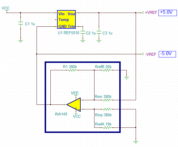
Figure 2: Using the INA149 for a dual-output precision voltage reference
For higher supply-voltage operations, you can build virtually any precision voltage reference using a reference option such as the REF5050 together with a high-voltage precision amplifier like the OPA192. By appropriately scaling the R1 through R4 resistors (Figure 3), you can split the nominal reference voltage of the basic reference block into any desirable parts. With the OPA192 maximum-input voltage offset of +/-25µV and drift of +/-0.5µV/C, you can ensure that the resulting precision voltage reference shown in Figure 3 maintains the initial accuracy and drift of the REF5050 basic building block provided that the required 0.01% matching of the ratios of the external resistors is not the limiting factor.
For linear operation of the circuit in Figure 3, the minimum positive supply of +1.2V is limited by the REF5050’s dropout voltage of 200mV. The minimum negative supply of -4.3V is based on the OPA192’s specified output swing of 300mV above its negative rail. The maximum positive supply of 14V is limited by the REF5050 maximum total supply of 18V, while the maximum negative supply can be as high as -34.8V (in case of Vcc = +1.2V) or -22V (for Vcc = 14V), limited only by the OPA192’s maximum total supply of 36V.
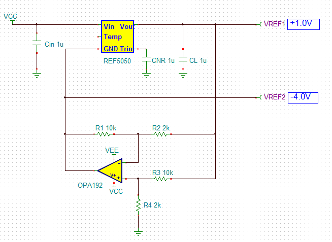
Figure 3: Using the OPA192 and REF5050 for asymmetric precision voltage references
There are a variety of ways to level-shift a precision voltage reference to virtually any required output voltage. However, one must take special care to properly choose not only external components like op amps, instrumentation amplifiers (INAs) and resistors, but also assure the minimum/maximum operating supply voltages so that they do not diminish the overall performance of the original circuit.
Additional resources
- Read R. Mark Stitt’s application bulletin on low power supply voltage operation of ref102 10.0v precision voltage reference
- Read other posts in the Understanding voltage references blog series.