

In part two of our Understanding Voltage References series, my colleague Christopher Dean talked about ultra-low dropout and how it is not just for the series reference. Today I’ll address how to achieve shunt reference flexibility with series reference precision.
A series voltage reference is a three-terminal device: VIN, VOUT and GND. It is similar in concept to a linear voltage regulator (LDO) but designed for a lower quiescent current and much higher accuracy. It may be thought of as the voltage-controlled resistance, VCR, between the VIN and VOUT. It regulates the output voltage by adjusting its internal resistance such that VIN minus the drop across the resistance, R, equals the reference voltage at VOUT; see the block diagram in Figure 1.
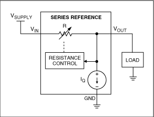
Figure 1: Series Voltage Reference - VCR Model
The series references generally have much better initial accuracy and temperature drift coefficient than do shunt references. Thus, if you need better than 0.1% initial accuracy and/or less than 25ppm/deg C temperature drift, you will most likely need a series voltage reference.
However, the shunt references offer more flexibility in terms of VIN range, as well as the option to stack multiple devices on top of one another to obtain higher reference voltages and the ability to create negative or floating references.
How can you combine the shunt reference design flexibility with series reference precision?
You can take advantage of the precision and stability characteristics of the REF50xx family by externally connecting the VIN and VOUT pins together. By doing so the series voltage references in this family are essentially converted into Zener diodes but with greatly diminished negative effects of shot noise and reverse-breakdown resistance. While any of the seven devices in this family could be used, I’ve selected here the REF5050 (5V output) and REF5010 (10V output) for my illustrations below.
The simplified schematic in Figure 2 shows the REF5050’s two main circuit components: BandGapAmp, with its gain stage responsible for assuring constant VOUT voltage over temperature and supply variations; and the ErrAmp output stage, capable of sinking or sourcing a minimum of 10mA output load current with minimal effect on output voltage initial accuracy.
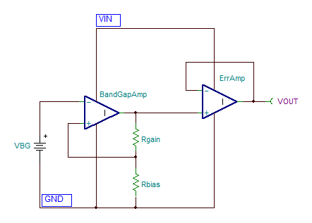 Figure 2: Simplified schematic of the REF5050
To assure VOUT initial accuracy and temperature drift, the class-AB output transistors must all operate in their linear region; thus, VDS must be greater than the transistor saturation voltage, Vsat. Therefore, the input voltage, VIN, of a series voltage reference must be at least a dropout voltage above VOUT; see the circuit in Figure 3. The dropout voltage is the minimum voltage difference between VIN (source) and VOUT (drain) under a given load, and in case of the REF5050, the minimum dropout voltage under quiescent condition (Iout=0) is 200mV.
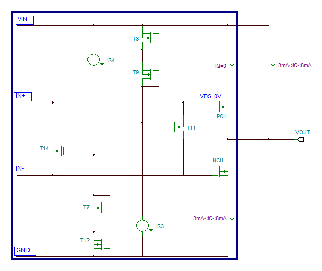
Figure 3: Placing REF5050 ErrAmp Output Stage in Shunt Configuration
However, by externally connecting VIN and VOUT together, as shown on the right in Figure 3, VDS = 0V and the upper output transistor, PCH, gets completely shut off. Under such conditions the output bias current, IQ, bypasses the PCH transistor entirely and flows directly from VIN to a lower output transistor, NCH. This establishes precision reference voltage between VIN and GND.
By shorting VIN and VOUT, the REF5050 is effectively transformed into a two-terminal shunt voltage reference, but it maintains the DC and temperature precision of a series voltage reference. Under this arrangement, the output stage biases up at a somewhat higher quiescent current than typical but the precision and stability of the REF5050 remain unchanged.
Figures 4 and 5 are examples of circuit configurations using the REF5050 and REF5010 as the basic building blocks.
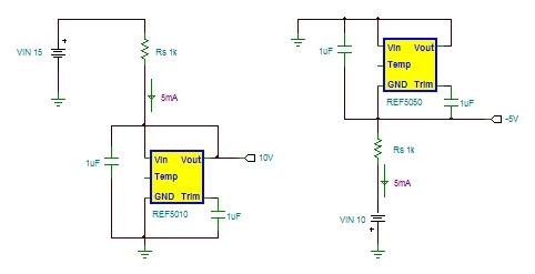
Figure 4: The REF50xx used in a positive and negative shunt configuration
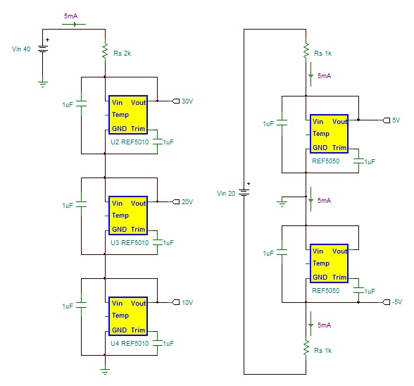
Figure 5: Stacking REF5010 for high- and REF5050 for dual-voltage shunt configuration
Given Rs is appropriately sized for required maximum output loading, using REF5050 or REF5010 as shunt reference, like shown above, imposes no limit on the maximum power-supply voltage since most of the voltage drop and power will typically be dissipated in Rs. Therefore, as a simple two-terminal device, REF50xx family of series voltage references configured as a shunt can be used in innovative circuits such as negative, dual and floating references. Additionally, multiple devices may be stacked on top of each other to obtain virtually any desired reference voltage.
The two-terminal application arrangement of the REF50xx has excellent characteristics which are closely related to an ideal Zener diode. The serial connections of REF5010 basic shunt blocks allow exceptionally high voltage references to be built (in thousands of volts) with very high voltage precision and superb temperature stability.
In part four of Understanding Voltage References, my colleague Chris Dean will explain how to use a shunt reference as a comparator.

Additional resources:
- Read Alexander Smolyakov and Mihail Gurevich’s “Stacking the REF50xx for High-Voltage References” application report.
- Check out this “Voltage Reference Selection Basics” white paper by Mario Endo.
- Read more posts in our “Understanding Voltage References” blog series.