

This technical article was updated on July 23, 2020.
Arguably the most important parameter that will determine the accuracy of your SAR ADC is settling error associated with the input and reference signals. “Well, what about the noise and linearity errors of the ADC?” you might ask. Good question, but if you’ve already picked a high-resolution ADC, then chances are these intrinsic ADC errors will be tiny compared to the settling errors associated with the ADC’s input and reference signal paths, if you’re not careful. In this post I will discuss how SAR ADC TINA models can be used to verify the settling characteristics of ADC input and reference drive circuits.
Perhaps the most important thing to realize about SAR ADCs is that their inputs are not high impedance ports. They contain switch-capacitor networks that draw load current from the input sources.
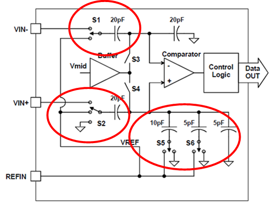
Figure 1: Rough SAR ADC schematic showing switch-capacitor networks at each input
The switches open and close at regular intervals. Each time a switch closes there are two kinds of loading phenomena that occur. First, there is charge injection from the internal analog switch. Second, there is a load current due to the charging/discharging of the internal capacitor. In both cases, the transient load current drops voltage across the non-zero output impedance of the input source and creates a transient voltage error. Figure 2 depicts a simplified model of this interaction between a voltage source and a switch-capacitor load for different values of source resistance.
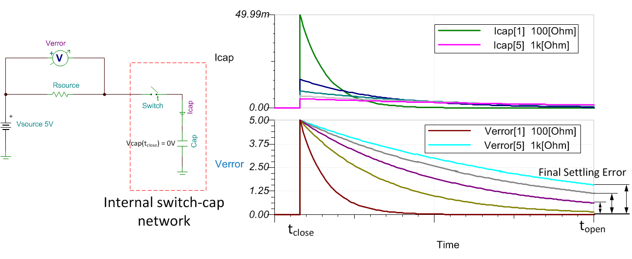
Figure 2: Simplified model of interaction between a voltage source and a switch-cap load
The voltage error settles more slowly as source impedance increases. Naturally, higher values of source impedance result in larger settling errors when the switch opens. For the ADC, this means sampling a wrong value of the analog input or reference voltage, and if the final settling error is > 1 LSB (“Least Significant Bit”), the ADC conversion result is inaccurate. For this reason, we need source impedance to be as low as possible when driving SAR ADC inputs. In fact, given that 1 LSB varies in inverse-exponential fashion with the ADCs (bits of) resolution (1 LSB = 1/2bits x full-scale input range), source impedance becomes even more critical for accuracy when you’re driving higher resolution SAR ADCs (all else being the same).
TI’s SAR ADC models accurately represent the loading characteristics of the input and reference pins so that users can test their drive circuits for settling accuracy. In fact, let’s use the ADS8860 TINA model to simulate the settling behavior of a few datasheet-recommended drive circuits – say, the ones recommended for processing full-scale step inputs at maximum sampling rate (see page 33 of the ADS8860 datasheet).
Figure 3 shows the settling behavior of the input drive circuit. Note that the reference (REF) pin driver has been replaced with an ideal voltage source in the interest of simulation speed and convergence.
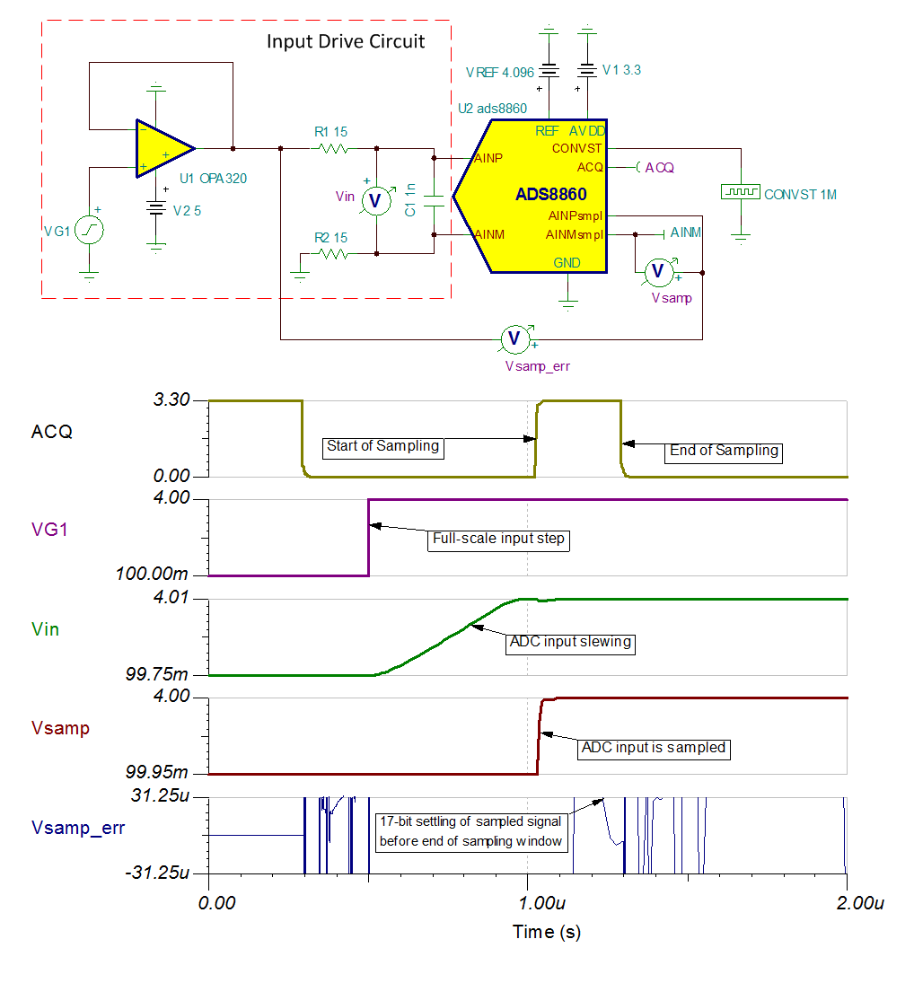
Figure 3: Typical simulation of settling behavior of SAR ADC input drive circuit
The “Vsamp_err” signal represents the transient error due to settling between the ADC input (“Vin”) and the sampled signal (“Vsamp”). Note that the transient error by the end of the sampling window in which the input step is acquired is less than ±31.25 µV or ±0.5 LSB in this case. This proves that the input drive circuit is able to drive the ADS8860 input with negligible settling error.
Similarly, we can verify the settling accuracy of the recommended reference drive circuit.
First we note the DC value of the ADC REF input:
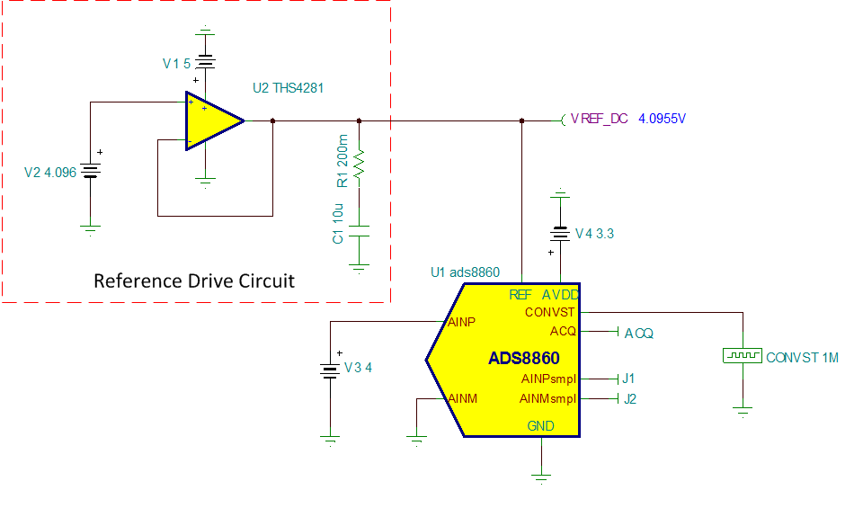
Figure 4: Simulation to compute DC operating point of ADC REF pin
Next we run a transient simulation and measure the transient error relative to the DC value:
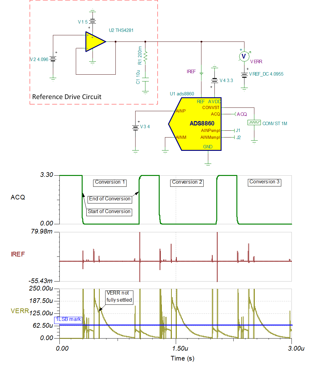 Figure 5: Transient simulation showing settling error of ADC REF pin over multiple conversion cycles
The “IREF” signal shows the spikes in load current whenever the ADC REF pin is sampled. Each disturbance creates a REF voltage error (represented by “VERR”). However, “VERR” settles to <1 LSB after virtually every load transient that disturbs the THS4281 output, except one instance where “VERR” settles to within 3 LSB, which isn’t terrible in terms of performance impact. Moreover, this may just be due to the conservative nature of our TINA models (ADC, or amps).
The next time you’re designing with TI Precision SAR ADCs, please be sure to take advantage of our SAR ADC TINA models to verify the accuracy of your input drive circuits before you commit to fab. Also be sure to check out our comprehensive collection of TI Designs for Precision Analog for a detailed look at optimizing your SAR ADC drive circuits for your application-specific needs.
Related resources: