

We use radio frequency (RF) communication in our everyday activities, whether calling a relative, texting a friend or even reading this blog post from a mobile device. There are many signals zipping through the air, but where do most of these signals originate? Most RF communication originates from cellular towers or wireless basestations such as the towers shown in Figure 1.

Figure 1: Mobile phone basestations
There are many components within these basestations, so a complete summary would turn into a Ph.D. dissertation! Instead, I’ll focus on one vital component to any basestation: the power amplifier (PA).
As you may have guessed, the purpose of a PA is to amplify low-power RF signals to the high-power RF signals driven into the basestation transmitter.
Before any RF signals are injected, a DC voltage (Vgate) is applied to the gate of the PA and adjusted until the desired drain current flows through the PA. This current is generally referred to as quiescent current – current that flows when no RF input is present. The quiescent current value is chosen to suit the end application, including the modulation scheme and device operation class. Figure 2 is a simplified schematic of a typical PA setup.
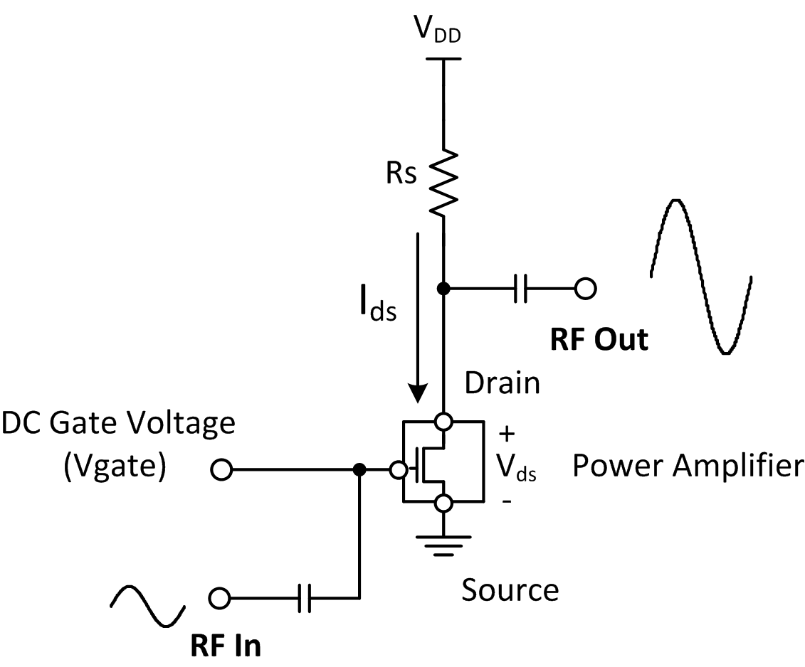
Figure 2: Simplified PA schematic
To better understand how the gate voltage and quiescent current affect RF (AC) performance, you can substitute the PA with a metal-oxide semiconductor field-effect transistor (MOSFET) model and derive the expressions below:
 (MOSFET in saturation) (1)
 (2)
(2)
Figure 3 is a graphical representation of both equations. A small RF input signal is driven onto the DC gate voltage, creating an AC drain current, ΔIds . This AC current oscillates around the quiescent current value, Idsq (Figure 3a). You can use MOSFET transistor I-V curves with load-line analysis to find the corresponding AC drain voltage, ΔVds (Figure 3b). In determining the relationship between AC drain voltage and AC drain current, equation 2 can further simplify to equation 3.
 (3)
(3)
Using the slope calculation of transconductance, gm , in Figure 3a, you can reduce the expression further to:
 (4)
(4)
Therefore the voltage gain of the amplifier, ΔVds/ ΔVgate, is defined as –Rs • gm , which translates to:
–Rs • 2 • Idsq/(Vgate – Vth)
The main takeaway from the expression above is that the gain for this configuration is directly proportional to the quiescent current, Idsq. Additionally, Idsq is chosen to ensure that the output voltage swing is not limited due to saturation; this is why you should select an Idsq value before RF operation, which requires a specific DC gate voltage.
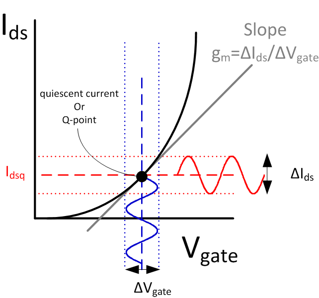
Figure 3: (a) MOSFET Vgate vs Ids graph
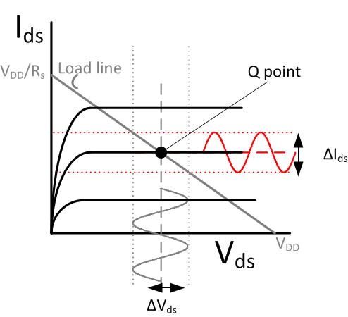
(b) MOSFET common-source load-line analysis
Traditionally, most PA biasing schemes use discrete solutions, some as simple as a potentiometer (variable resistor divider) on the gate of the PA. Newer methods leverage the accuracy and digital interfaces of precision digital-to-analog converters (DACs) and/or digital potentiometers. Different PA technologies, such as laterally diffused MOSFET (LDMOS), gallium arsenide (GaAs) and gallium nitride (GaN), require different levels of gate voltage for device operation. For example, GaN and GaAs require negative-biasing schemes, while LDMOS requires a positive voltage for device operation. For this reason, many PA biasing solutions are now starting to include DACs with bipolar ranges.
PAs display nonlinearities during device operation that are mostly dependent on temperature. These nonlinearities significantly impact performance, as they result in unpredictable device behavior. Stay tuned, as I’ll discuss these nonlinearities in future posts.
For more information about PA biasing solutions or analog monitoring and control (AMC) devices, check out these products: AMC7812, AMC7832, AMC7836.