

Everyone knows that op amps should have power supply bypass capacitors located near the IC’s terminals, right? But why? Why, for example, is an amplifier more apt to oscillate without proper bypassing? The reasons will increase your understanding and awareness.
Power supply rejection is an amplifier’s ability to reject variations in the power supply voltage. Figure 1, an example, shows that this rejection capability is very good at low frequency but diminishes as frequency increases. Hummm... poorer rejection at high frequency where oscillations occur?
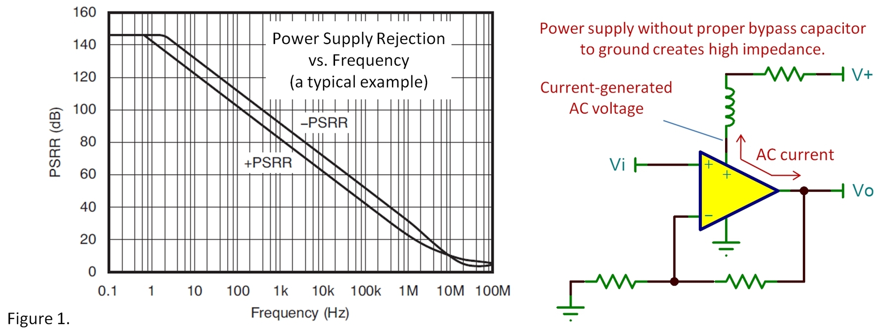
We often think of external power supply-borne noise interfering with an amplifier. But op amps can create their own problems. For example, output load current must come from the power supply terminals. Without proper bypassing the impedance at a supply terminal can be high. This allows AC load current to produce an AC voltage on the supply pin. This creates an unintended, uncontrolled feedback path. Inductance in this power supply connection can magnify the resulting AC voltage at the supply pin. At high frequency, where power supply rejection is poor, this unintended feedback can cause oscillation.
There are internal forces at work, too. Without a solid power supply, internal circuit nodes may talk to one another creating unwanted feedback paths. Internal circuitry is designed to operate with firm, low impedance on the power supply terminals. An amplifier may behave quite differently and unpredictably without the solid base of low impedance supplies.
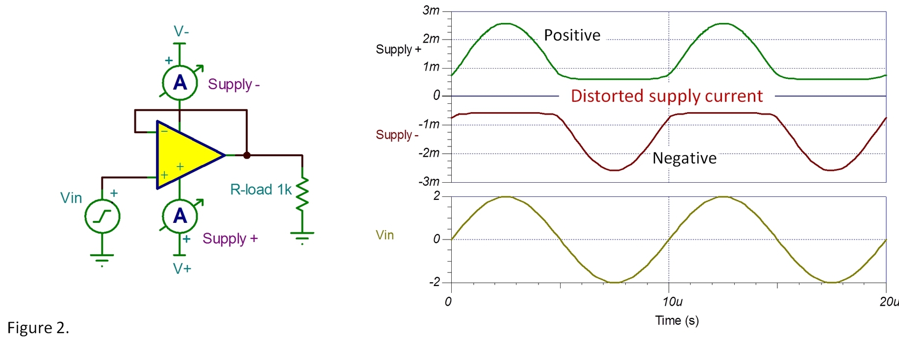
With a clean sine wave input, the unintended feedback due to poor bypassing may not be a tidy sine wave. The signal currents in the supply terminals, figure 2, are often highly distorted because they only represent one half of sine wave current. With different power supply rejection characteristics on the positive and negative supplies, the net effect will distort the output waveform.
The issues are magnified with high load current. Reactive loads create phase-shifted load currents that may exacerbate issues. Capacitive loads are already at higher risk of oscillations due to additional phase shift in the feedback path (more detail here). These higher risk cases may need higher value tantalum bypass capacitors and extra care in circuit layout, compact and direct.
Of course, not all poorly bypassed amplifiers oscillate. There may not be sufficient positive feedback, or the phase not quite right (or wrong!) to sustain an oscillation. Nevertheless, performance may be compromised. Frequency and pulse response may be affected with excessive overshoot and poor settling time.
As discussed in a previous blog, these behaviors are not well-modeled in TINA-TI or other SPICE programs. Voltage sources in SPICE are perfectly solid, unperturbed by load currents. Modeling the actual source impedance of your supply and board layout with additional components is tricky and imprecise. Power supply rejection magnitude is modeled in our best macro-models, but the phase relationship of this feedback path is unlikely to match reality. Simulation can be tremendously useful but won’t accurately predict this behavior.
All this should not cause you to be paranoid—no need to go crazy with bypassing. Just be alert to particularly sensitive situations and signs of potential problems. Good analog design thrives with a healthy dose of understanding and awareness. :-)
Thanks for reading and comments are welcome below.
Bruce email: thesignal@list.ti.com (Email for direct communications. Comments for all, below.)
Look here… 55+ other interesting technical topics The Signal blogs.
-

John Davies
-
Cancel
-
Vote Up
0
Vote Down
-
-
Sign in to reply
-
More
-
Cancel
Comment-

John Davies
-
Cancel
-
Vote Up
0
Vote Down
-
-
Sign in to reply
-
More
-
Cancel
Children