

We’ve included device-level ESD performance of our ICs in data sheets for many years. But these figures apply to an integrated circuit before soldering onto your circuit board. What about ESD tolerance on your PCB?
We qualify the ESD performance by zapping each pin multiple times on several devices. It simulates nasty mistreatment that might occur during handling and assembly. Without internal ESD protection circuits, damage could occur with static charges as low as 10V.
But you’re also concerned (maybe more concerned) with ESD tolerance after PCB assembly and during operation. An IC is generally much more robust after assembly on a circuit board. Power supply connections have bypass capacitors that can absorb sizable discharges. Input and output connections to the board generally have series resistance and PCB trace inductance. Capacitance to ground, even if only from the PCB trace, increases the ability to absorb a static discharge without damage.
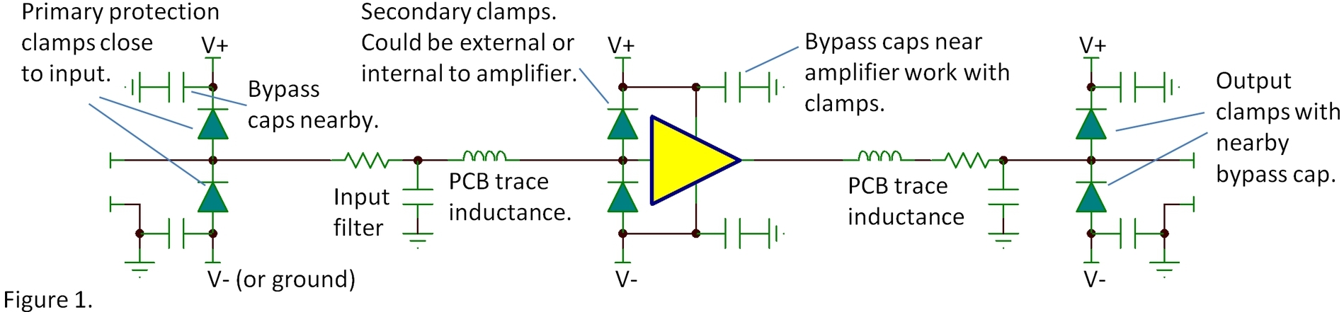
You can add additional diode clamps or zener-like protection devices1 that will greatly improve ESD tolerance of your complete product or equipment. Figure 1 shows a basic approach—and more information here.
This is about survival of your circuitry but you should also consider functional disturbances. This might include gross overloads of analog circuitry that require a long recovery time. Scrambled bits in digital circuitry or the system processor could be an even bigger problem. You probably cringe as I do when you draw a static spark as you touch your PC. Even though there may be no permanent damage to the hardware, an ESD “hit” can cause a system reset or lost data. You, with analog skills, may be the best person to guide the PCB layout, system layout and grounding to assure your system or product can withstand a zap without lost data or reboot.
Deliberate planning and execution will help achieve good results. Think about where the current flows during a static discharge. Consider both polarities of current flow to assure a safe current path.
It’s best to confine the discharge current path close to entry point. A discharge to the input ground terminal should find an easy path to earth ground without snaking around your circuit board. Keep the current path away from parallel lines that could be disturbed by capacitive or inductive coupling. A discharge to the input terminal must find a current path to ground. The diode clamps shown in figure 1 provide a short path to the power supplies, then through the bypass capacitors to ground.
Consider the same issues for an output terminal or any other likely point of conductive contact with your product or equipment.
With careful design and thoughtful PCB layout, you can improve the ESD tolerance of your system, including survival and functional tolerance. If you have big problems, we have an expert available for consultation. Jae Park has helped numerous customers sort out difficulties in their boards and systems. Reach him through our E2E forums specific to the product type relating to your issues.
Have you solved a tricky ESD sensitivity problem? Tell us how, below.
Bruce email: thesignal@list.ti.com (Email for direct communications.)
Check out other interesting topics… Table of Contents for all The Signal blogs
Note 1) In a prior blog on EOS protection, I lamented that many protection devices had too much leakage current for many precision circuits. These new 5V protection devices have lower leakage.
-

Bruce Trump
-
Cancel
-
Vote Up
0
Vote Down
-
-
Sign in to reply
-
More
-
Cancel
Comment-

Bruce Trump
-
Cancel
-
Vote Up
0
Vote Down
-
-
Sign in to reply
-
More
-
Cancel
Children