I’m surprised by the number of questions we get on our support forums regarding photodiodes and associated circuits. Here is a 10-minute quick-start—the stuff an analog designer should know.

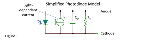
A simple photodiode model shows the key elements—a diode in parallel with a current source that is proportional to the irradiance (light intensity).  Parasitic components CD and RD can play a role in performance.

Photovoltaic Mode—the photocurrent flows in the circular path shown in figure 2, forward biasing the diode.  The unloaded output voltage has a nearly logarithmic relationship with the photocurrent according to the diode’s logarithmic forward V-I characteristic, modified at very low current by RD. So the output voltage is highly nonlinear with irradiance. This can be a benefit in some applications because the perceived change in “brightness” of the light (the eye is pretty logarithmic) produces a similar change in voltage throughout a wide range. The absolute relationship of voltage to irradiance is poor due to the temperature dependence of the diode’s V-I characteristic.

Diode capacitance limits frequency response in photovoltaic mode. Rapid changes in irradiance must charge and discharge CD. This is not the mode to use for fast response.

The output can be buffered or amplified with a simple non-inverting op amp circuit. Use a CMOS or JFET op amp for low input bias current so you don’t load the photodiode at low irradiance levels.

To generate power in photovoltaic mode, the output is loaded and the voltage sags significantly. The loading for highest power output depends on the irradiance.

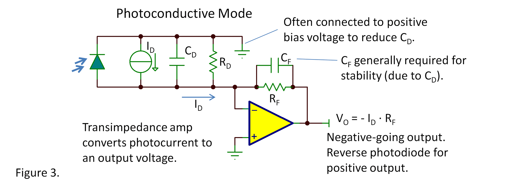
Photoconductive Mode—the diode voltage is held constant, often at 0V as shown in figure 3. A transimpedance amplifier (TIA) is commonly used to convert the photocurrent to a voltage. Reverse bias can be used on the photodiode to reduce its capacitance but this creates a dark current leakage. With no forward voltage developed on the diode, the response is very linear with irradiance. Furthermore, the voltage across the diode capacitance does not change with irradiance so frequency response is greatly improved. Low capacitance is still important because it creates a pole in the feedback path. This generally requires a feedback capacitor, CF, for stability.

You can get some of the benefits of photoconductive mode simply by loading a photodiode with a low value resistor, say around 50 ohms. If the diode voltage does not exceed 20mV, or so, you do not significantly forward bias the diode and response is reasonably linear and fast. Sensitivity, however, is low.

Avalanche Photodiodes are special types designed to operate with a high reverse bias voltage, nearing the diode’s breakdown. This provides amplification of the output current at low irradiance.

Selecting a photodiode can have many tricky tradeoffs involving photodiode size, capacitance, noise, dark current leakage and package types. In general, it’s best to use a small photodiode and concentrate a limited light source with a reflector or lens. TI does not make solo photodiodes but for many basic applications the OPT101 provides a complete solution with photodiode and TIA on the same IC.

Sorry, that was a concentrated spew. There are engineers who make their careers designing photodiode circuits and there’s much more to know for high performance applications. But you’ve seen most of what I know so I’m not an authority on the subject. In fact, you could say that of most all my topics. It’s the reason I write blogs, not books.

Thanks for reading. Have you used a photodiode for an unusual purpose? Tell us. Experts are welcome to offer additional comments or suggestions.

Bruce          email:  thesignal@list.ti.com

           Index to all The Signal blogs.

Anonymous
  • Readers—I’ve condensed a series of emails with Barry, an engineer with significant photo-electronic experience. He had comments on the issue of photovoltaic vs. photoconductive modes:

    [Barry] I was thinking that one should use the term 'current-sourcing, or 'photo-current mode' for the TIA, with 'forced zero voltage', since the diode is not conducting with light input, it is sourcing a current ... in the reverse-biased mode, I think that we actually see something that looks like increasing conductance with increasing light level? Just an idea to think about, so that one has three discrete, and descriptive, terms for the three application modes?

    [Bruce] You have a sensible proposal--one that makes great sense if we were starting from zero to write literature on the subject. The problem is that there are so many existing references on photodiodes that describe the two regions of operation, leaving the forced zero voltage case in the ambiguous middle. I actually think "photoconductive" is a bit of a misnomer. In my mind, the "conduction" is really not like a passive photo-resistive cell, it's the same photo-generated current that occurs at zero volts. We've just applied a bias on the diode. The magnitude and behavior of the current is the same (except for dark current, the leakage of the diode).

    [Barry] Indeed... I guess that we could view the zero-voltage mode is just a special case of reverse-bias...in fact, I think that the load lines look the same, as long as the internal diode is not 'turned on', even for bias voltages above zero. AH, terminology; I'm active on a CIE standards committee for LED terminology, and trying to harmonize with the IEC terminology, which is quite 'old-tech', is difficult, at times.

    [Bruce] Yup, the load lines for constant voltage are the same, even with a small constant forward bias. It requires some forward conduction of the diode to alter the load line.

    [Barry] It seems that there is, actually, a continuum in 'modes', with the difference being the beginning of forward conduction of the diode, and the increase in response speed due to the induced changes in the depletion region.

  • Thanks for your comments, Bonnie. After speaking with you and more reading on various web sites, I see that there is conflicting information and some confusing semantics on this point. Does "zero bias" mean zero voltage or unloaded? Same for "unbiased," the terminology used in some literature. And frequently the zero voltage condition is not clearly described.

    My point would be that a TIA with zero voltage across the photodiode has a transfer function that is nearly identical to a fully reverse-biased photodiode. It requires a substantial and variable forward bias to clearly enter the characteristic V-I region of photovoltaic mode. Furthermore, a zero-biased TIA does not "allow a voltage build up" as described in your quoted literature.

    Taking the opposite side, however, some of the more subtle changes associated with reverse-bias photoconductive mode such as reduced capacitance, inception of dark current and increased noise require a reverse bias. These changes in behavior can be very important in high-performance applications and this may be a good reason to reserve the photoconductive designation for reverse biased conditions.

    Okay, photodiode experts... this is your chance to weigh in!

    Bruce

  • I love your blog column and it looks like customers are very interested in it as well. Very nice Blog!!!

    I was reading through your photodiode blog (just published three days ago) and I am running into some confusion about your definition of photoconductive versus photovoltaic. I am not familiar with your photovoltaic circuit and I am also not finding it in any other literature. But going on, your photoconductive circuit is actually a combination of photovoltaic and photoconductive circuits. If you apply the bias voltage (which you do have a comment in the circuit about) then you have a photoconductive circuit. If you ground the diode cathode you have a photovoltaic circuit. The definitions of these circuits that I find in literature are:

    Photovoltaic: When used in zero bias or photovoltaic mode, the flow of photocurrent out of the device is restricted and a voltage builds up. This mode exploits the photovoltaic effect, which is the basis for solar cells – a traditional solar cell is just a large area photodiode.

    Photoconductive: In this mode the diode is often reverse biased (with the cathode positive), dramatically reducing the response time at the expense of increased noise. This increases the width of the depletion layer, which decreases the junction's capacitance resulting in faster response times. The reverse bias induces only a small amount of current (known as saturation or back current) along its direction while the photocurrent remains virtually the same.

    I don’t know how I have gotten confused on this issue.Please help.