

Did you see last week’s resistor puzzle? Check it out if you missed it. Here’s the solution:
We’re not accustomed to reading three-dimensional schematics so the first step is to redraw it clearly. There are three distinct paths from A to B, colored blue, green and red. Each has a series connection of 1Ω—R—1Ω. The 3Ω resistors are effectively in parallel with the “R” resistors. The symmetry of these 3Ω resistor connections makes their effect the same as if each is directly in parallel with one of the “R” resistors.
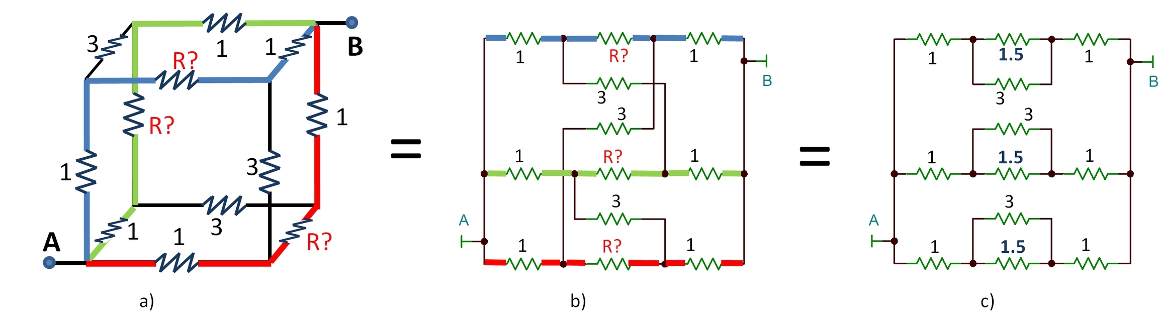
The total resistance from A to B is 1Ω, so each of the three legs must be 3Ω. With 1Ω on each end of the legs, the middle parallel combination must also be 1Ω. So R must be 1.5Ω in parallel with 3Ω to make 1Ω.
Was this fun? Maybe you missed a previous puzzle, the infinite resistor network. More fun.
It’s all so much easier when we have a well-drawn schematic. Huummmm… a well-drawn schematic?
A genius former colleague in my past used to say “circuits work better when the schematic is drawn right.” He didn’t mean “drawn without errors.” He meant that it was easier to understand the circuit when it was drawn well. Nuances are easier to discern, details more easily optimized and problems are more easily resolved. So true!
I’m on my soapbox now! Have pride in your schematics. A well-designed circuit deserves a well-drawn schematic. And a poorly drawn schematic does not inspire confidence in your work.
Take care in laying out your schematic. Signals flow better left-to-right, you know. Currents flow downward. With thoughtful layout, you can minimize confusing crossovers and labeled interconnections that hinder interpretation. If you need multiple pages, make connections clear, preferably so one sheet can lie next to another and connections are obvious. Draw sub-circuits the same way each instance they occur so they are easily recognized.
Use familiar symbols. Op amps are triangles not rectangles—much easier to read this way. When possible, place components in a way that suggests a good circuit board layout. Draw symmetrically if this is desirable in the PCB layout. Label IC part numbers and include all circuit values. Number components so that they can be identified easily in e-mails or phone conversations.
So often, I see schematics without a single word of helpful annotation. A few words of explanation can add so much! A footnote explaining why a certain component is chosen or how a value is calculated can be so valuable to a support engineer a few years later. How about labeling some nominal voltages at key nodes? Show gain values and nominal signal levels. Label major blocks. If you last as long as I, you may be the beneficiary of your own good documentation as you retrace your own steps.
Some thought and empathy will make life easier for those who later must decipher your circuit. Make the quality of your schematics a signature feature of your excellent work. Oh, yes… signature! A valued colleague here at TI insists that you should put your name on your schematic. (Thanks, Jim.) You may find that this simple act will cause you to recheck your work one last time. ;-)
Schematics… what’s your pet peeve? What’s your rant? Leave your comments.
Thanks for reading,
Bruce email: thesignal@list.ti.com (Email for direct communications. Comments for all, below.)
Check out 50+ interesting topics… Table of Contents for all The Signal blogs.
-

Mike Kaelin
-
Cancel
-
Vote Up
0
Vote Down
-
-
Sign in to reply
-
More
-
Cancel
Comment-

Mike Kaelin
-
Cancel
-
Vote Up
0
Vote Down
-
-
Sign in to reply
-
More
-
Cancel
Children