This thread has been locked.

If you have a related question, please click the "Ask a related question" button in the top right corner. The newly created question will be automatically linked to this question.

UCC25660: UCC256601DDBR Doesn't Start Up.

Part Number: UCC25660


Tool/software:

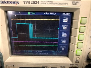
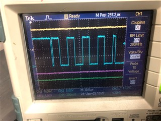
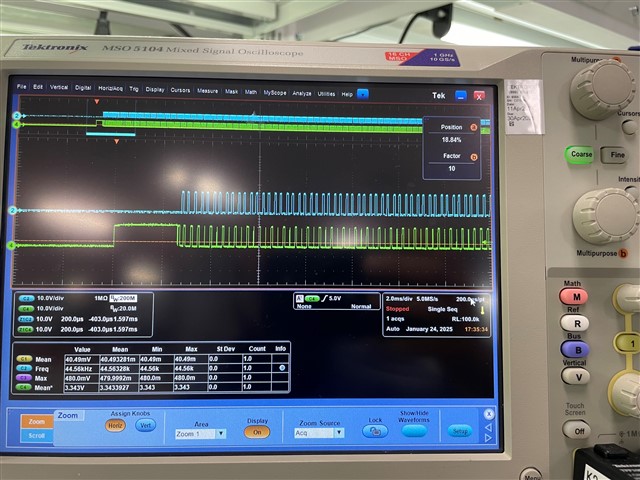
Similar schematics for LLC converter as Alex Drobyshev posted recently except that I use a separate source for AC voltage for HV startup but nonetheless my UCC256601 never started. What I can see is 7.9 to 8 VDC on pin12 for VCC (EVM shows 12VDC) and no 5VDC on pin 8 for V5P. With an oscilloscope I can only see there 1volt square shape pulses, 120ms long with a period of about 1200ms on pin8 for V5P. When I tried to reduce AC voltage supplied from an isolated transformer to pin1 for HV, the frequency for those pulses increases also but their magnitude remains the same at 1V level. VCC voltage does not change, it stays at about 8VDC level. When the power was turned off surprisingly those pulses stay for a very long time, about 10-20 minutes. Some large capacity discharging at very low consumption rate? I checked all components connected to V5P, nothing that can overload it during start up. TSET resistors are 1000K/200K for Upper/Lower. LL resistors are 600K/150K respectively. C10 is 4.7uF. C13 is 1uF ceramic capacitor. OTP programming circuit connected not to Vin as Alex shows but to Vcc as suggested in EVM schematics. What could be wrong that prevents the HV startup?

  • Are you working with Alex Drobyshev together? It would be better to consolidate the inquiry together.

    We will take a look and get back to you.


  • No, I'm not working with Alex Drobyshev. I just found his topic recently on the forum and asked related questions. I don't mind consolidating them. While waiting for a reply I investigated my PCB further and tried a few options. I disconnected both programming dividers for TSET and LL from V5P and still not found 5VDC on the pin 8. With 120VAC rectified and through 5K resistor connected to HV the VCC voltage is firmly at 8.0VDC and I can see 1volt pulses on Pin8 as I described earlier. I also tried to supply VCC from a separate DC power supply with 8VDC and then 15VDC to check if 5VDC will appear on V5P but with no success. Just 1volt pulses with a frequency which depends solely on the voltage on HV pin. My understanding is that it stuck when it reaches configuration setting time and does not go any further for some reason (because there is no 5VDC on V5P?). Just minutes before I got Ning Tan questions, I decided to replace the UCC256601 chip because I suspect it (LDO?) might be damaged. Please let me know your opinion.

  • Hi Viktor,

    After replaced with the new IC, are you able to see V5P? Could you share your schematics?

    Regards

    Manikanta P

  • After replacing with new IC I was able to see 5 VDC at Pin8 for V5P and 12 VDC at Pin12 for VCC. Everything was normal, the same as I can see on the evaluation module. However, when I applied main power at input voltage of about 285-287 volts something happened again and the situation returned to where it was before with the previous IC: 8VDC at Vcc Pin12 and the same 1.2 volts pulsing pattern on V5P pin 8. I assume the new IC is dead again. 

  • A new IC soldered in instead of the failed one. 120VAC connected and both V5P and VCC voltages are OK again. Any suggestions on how to proceed ahead will be appreciated. My schematics attached in a pdf file above. All programming resistor values are from TI "excel design calculator" for UCC25660.

  • Hi Viktor,

    Could you change the boot cap from 1uF to 100nF and see if that helps avoiding the failure.

    Regards

    Manikanta P

  • I actually started with 100nF for the boot capacitor with my first attempt and then when it did not start, I increased it to 1uF. I can certainly come back and try again. My current thoughts are that failure might happen during the first attempt to open MOSFET which returns about 1/10th of Vin value through the bias coil on the transformer to Vcc and also to OVP/OTP pins. The max voltage for Vcc is 30VDC while for Pin4 it is only 5.5VDC. Is this a real concern? Do I need a Zener there to limit that voltage at let's say 15 volts? Please let me know.

  • Hi Viktor,

    You need to use zener or voltage regulator to restrict the VCCP voltage below 18.5V.

    Regards

    Manikanta P

  • Thank you for comments on Zener for VCC. Before I was able to read your message, I found an error in my PCB where R11 instead of 51K was by mistake 42.2 Ohms (same value as R6) for the lower MOSFET gate circuit. I replaced the resistor and checked both MOSFETs - they were fine. I applied 120VAC - both V5P and Vcc voltages were normal. Then I applied Vin and increased it gradually from 150VDC to somewhere below 300 volts when I found that Vin is shorted. I turned Vin OFF and noticed that V5P and VCC were OK this time. But both MOSFETs are dead now. I was not able to catch the moment to see if there were any pulses on Pin11 or 15. Perhaps they both opened at the same time? How can I test pulses on Pins 11 and 15? What do I need to do to simulate switching conditions without use of Vin or powering MOSFETs? If I apply let's say 15VDC to VCC will the switching start or do I need some other input signals like BLK and HV (what else?) to be present too? Thank you.

  • Hi Viktor,

    You can apply VCC of 15V and then apply BLK of 1.2V directly at the pin. Then you should see the pulses at the gate signals of the IC. While following this method, you don't need to apply HV or high voltage DC input.

    Regards

    Manikanta P

  • With VCC of 15V and BLK of 1.2V applied from external power supply I can see V5P of 5VDC. Output Pin15 is at 10VDC with no pulses at all while Pin11 has rare pulses (more than 1s period) of 15V with about 100us length followed by a few short pulses less than 10us long. Is that a sign of a burst mode or something else? 

  • Hi Viktor,

    Here is what I am seeing at the LO and HO signals when I apply BLK 1.2 and VCCP of 15V.

    Its restarting every 1sec.

    Regards

    Manikanta P

  • Thank you. Apparently, I have some problem with HO. I will continue investigation next week. What is that 120us long pulse for at the beginning? 

  • Its the boot charge period which is around 265us.

    Regards

    Manikanta P

  • Thank you, that's helpful.

  • No, we don't.
    I started to read again all threads, related to the chip, with intention to find out how other users succeeded with running this chip and suddenly found this thread.


  • Alex,

    Thanks for the clarification.

  • Hi Victor, I'm happy (and not) to find fellow, facing same issue like me. :)

    What I can add from my side, regarding the 8V at the PIN12.
    I used wrong version of the chip (__01 with X-cap discharge functionality), but fed it by the 380DC.
    I also was observing 8V at the Vcc pin, during applied 380VDC.
    8V could be flat line, or contain some triangular pulsation, I couldn't find what causes change in the voltage shape.

    The same time, 5V could be available or not.
    I was advised by Manikanta about wrong understanding of the chip's details, so I got __02 version, without "X-cap discharge", but never used it with HV current source, only with external laboratory PSU (HV series resistor depopulated).
    Still I facing troubles with V5P.
    5V can appear, stay stable, but in case of Vcc voltage ON-OFF-ON, it collapses and never returns back.


  • >>How can I test pulses on Pins 11 and 15?

    I would like to alert you about measurement at the PIN15 to PIN16, if you will want to do that to check the Gate-Source pulses shape.
    You should avoid connecting oscilloscope GND  to the PIN16 (HS), it will cause driver failure with very high probability.
    To measure PIN15-PIN16 you have to use differential probe.

    You can use ordinary HV probe, with 100:1 division factor, to check if there are pulses at the HO pin, respectively to the GND.
    Amplitude of the sensed voltage will be equivalent to your Vcc+Vdc.

  • A long pulse at the LO pin is needed to let the Cboot charge to the Vcc voltage, through the Rboot resistor.
    This long pulse should be present during each power converter startup.
    After that, the long pulse is no longer required, as Cboot will be charged, and short pulses times will be sufficient to replenish Cboot charge lost during MosFet gate charging.

  • Hi Alex, thank you for coming back to the discussion. Yes, I make all measurements relative to the ground, I realize that HS could be as high as Vin. Long story short, after replacing the IC two times and replacing both MOSFETs I came to a conclusion (wrong or right) that most likely I have an issue with parasitic capacitance and/or inductance of my prototype board (I do not have better explanation of how I shorted both MOSFETs). I was able to see gate pulses with external 15VDC (same as Manikanta's above) but then when I applied Vin at only 80VDC the switching picture becomes extremely noisy and HS pin potential was fluctuating to over 250V. With Vin at 280VDC it probably can kills my 600V rated MOSFETs. I left these tests there for now and, to do everything right, I decided to start working on a new layout for PCB using KiCad which is something new for me and I have to learn.

  • Hi Viktor,
    Once I destroyed both MosFets what I shorted CS sensing resistor.
    So power stage started to develop current amplitude higher and higher, till the first MosFet fails. Then, second MosFet fails due being opened by driver.

    The second point.
    Do not use your oscilloscope with its GND connected to half-bridge middle point.
    HB mid point switches between zero level and high voltage level, and your (oscilloscope_to_ac_grid_capacity) is connected to that point.
    You can try to use battery powered oscilloscope, placed onto insulated island, perhaps it will work.
    But the appropriate approach is to use differential probe for measuring HB mid point to HI gate.

  • Hi Alex, I was able to observe HO pulses clearly (as well as LO) when I had both MOSFETs yet shorted (before I replaced them) with no Vin power, but after replacing the shorted MOSFETs I can find only LO pulses, until I applied Vin which opened lower MOSFET to do the boot up cycle, as I understand.

    I connected my oscilloscope relative to the ground for all my measurements. I started with a safe low Vin level and increased it gradually up to 80VDC and this is where I noticed that HS potential already exceeds 250 volts. Switching frequency was about 340kHz but all signals were very noisy, hard to sinchronize. I decided to stop there to upgrade my PCB. I suspect that at Vin of 280 volts HS voltage went over 600 volts limit for MOSFET. Power supply for Vin supposes to limit current at 1 amp (CV/CC mode setting) but nevertheless both MOSFETs were shorted the moment switching started.

    Thank you for comments.

  • You can start with no HV voltage at all.
    The chip will start working with 16V applied to Vcc pin.
    You can use oscil. referenced to GND, observe both LO and HO pulses.
    HO pulses amplitude in this case should be 2xVcc voltage.
    This is safe way to check that driver works properly, and all yours service circuits connected to V5P work correctly.

    In my case, I facing troubles with V5P 5V voltage establishing.
    Something goes wrong and 5V appears only as pulses.
    You can check my topic to see updates.

  • When I replaced IC it solved my problem with not having 5V at V5P. I got that 5V with 15V to Vcc or 120VAC to HV pin. Not sure what was going inside the IC but when I observed just 1volt pulses there going every second I thought that the IC is dead and replaced it. It happened a couple of times with me.

    As I said earlier with no Vin voltage I was able to see output pulses on LO output very well but nothing on HO (just tiny remnants) when I put new MOSFETS in. Only when both MOSFETS were shorted (dead) I was able to see good 15volt pulses on HO relative to the ground (without Vin).

  • I was able to see good 15volt pulses on HO relative to the ground (without Vin).

    Let's check again.

    In case of operational MosFets, with applied 100VDC voltage, your HO signal amplitude should be DC+Vcc = 100V+16V=116V
    So you might be overload your oscilloscope input, though signal was shown over a the screen limit.

    In case you have shorted BOT (or both) MosFets, shorted BOT MosFet's drain is connected to the GND, thus your bootstrap driver will not "boost" its voltage, "stored" in Cboot over the HV one, it will only open its internal switch and you will see pulses with Vcc amplitude.


  • Viktor, check Rboot resistor.

    Resistor limiting charging current for the Cboot.