This thread has been locked.

If you have a related question, please click the "Ask a related question" button in the top right corner. The newly created question will be automatically linked to this question.

TPS56A37: Question on using parallel-switched bottom feedback resistor to select 5 V / 12 V outputs

Part Number: TPS56A37

Tool/software:

Dear TI Support Team,

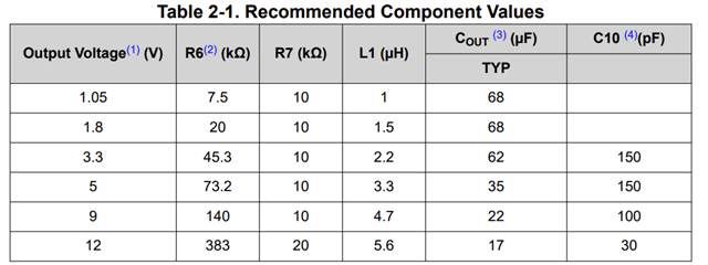
I’m designing with a TI buck regulator whose datasheet/EVM table lists example feedback resistor pairs (R6 top / R7 bottom) for various output voltages. I understand those values are recommendations rather than fixed requirements, as VOUT is set by the divider ratio.

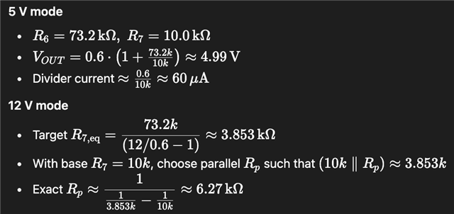
For my application, I would like to select between 5 V and 12 V by switching the bottom feedback path (R7) with a MOSFET in parallel:

Before I finalize this approach, I’d appreciate your guidance on the following points:

  1. [General Validity]
    Is it acceptable to deviate from the resistor values shown in the table as long as the divider current remains in a reasonable range (e.g., a few tens of µA to ~100 µA) and VOUT is correct?

  2. [Inductor selection]
    For the inductor, the guide recommends 3.3 µH for a 5 V output and 5.6 µH for a 12 V output. In this case, is it acceptable to use 5.6 µH for both outputs?
    (or.. is 3.3uH Okay? - I want to use 3.3uH for cost efficiency) 
  3. [Transition Behavior]
    When switching from 5 V to 12 V (or vice versa), do you recommend disabling the converter via EN first to avoid output glitches, or is it acceptable to switch R7 in-circuit if we limit the gate slew (small RC on the MOSFET gate)?

  4. [Compensation / Cff Interaction] - Cff is specified in the datasheet schematic.
    If a feed-forward capacitor (Cff) from VOUT to FB is used per the datasheet, should we retune Cff for the two output settings, or is a single value typically adequate for both 5 V and 12 V with this device?

I plan to prototype both modes and validate stability (phase margin) and transient response at VIN min/max and full load. Any additional best practices or application notes you can share would be greatly appreciated.

Thank you for your support.

  • Hello,

    Let me check and get back to you.

    -Hitesh

  • Hello,

    1. Yes you can use this configuration, but dynamically changing the output resistor is not recommended as the converter susceptible to noise

    2. this depends upon the ripple current and Vout ripple voltage,  I can suggest to keep the L*C product within the maximum and minimum suggested values.

    3. for slower slew rate you can check individually, but TI doesn't recommend to change it dynamically.

    4. Optimizing Transient Response of Internally Compensated DC-DC Converters (Rev. B) refer this to tune the Cff or try with 100pF as its common for both.

    -Hitesh

    1. If I change the feedback resistor values after turning off the buck DCDC converter via the EN pin (i.e., not during active output), is there any issue with this approach?

    2. Regarding your previous answer: does it mean that even for a 12 V output, I can use a 3.3 µH inductor instead of 5.6 µH if I increase the output capacitance (CAP)?
      If so, could you recommend an appropriate CAP value for a 12 V / 4 A output when using a 3.3 µH inductor?

    Just to clarify: I do not intend to change the output voltage dynamically.
    I plan to turn off the converter first, then change the feedback resistor divider, and only then re-enable the output.
    I’d like to confirm if this method is acceptable.

    Thank you

    -Hyungjune choi

  • 1. No issues with this you can try it out.

    2. Can you try out 4.7uH Inductor and 47uF 25V capacitor.

    Recommended to check the frequency response for both the output voltages as we are trying components with between 5V and 12V output values

    -Hitesh

  • I think the real reason you recommend 4.7 µH instead of 3.3 µH is to minimize entry into DCM, right?
    In my application, the maximum load is 5 V / 10 A or 12 V / 4 A, but in reality the load can swing all the way down to 0 A.
    For example, it might operate at 5 V / 0.5 A or even 12 V / 0.1 A.
    So inevitably, I’ll enter DCM no matter what.

    If I just accept DCM operation, would it be fine to use 3.3 µH with four 22 µF capacitors on the output side?

  • Hello Hyungjune,

    The recommended values are in accordance with the internal loop compensation parameters, hence I would think of minimum deviation for the ideal values.

    If cost optimization is the issue you can try with 3.3uF, and check the stability of the system by checking bode plot for each load and make sure you have sufficient PM and GM.

    -Hitesh