A related question is a question created from another question. When the related question is created, it will be automatically linked to the original question.
If you have a related question, please click the "Ask a related question" button in the top right corner. The newly created question will be automatically linked to this question.
[FAQ] TDA4VM: How to identify a GPIO and toggle the same
Please follow the below steps to configure WKUP_GPIO0_x as output. The steps below are for TDA4VM. The similar steps could be followed for other Jacinto devices.
I shall take an example of WKUP_GPIO0_6 (Test point 45 (TP45) on J721EXCP01EVM)
1. Select a GPIO that has TP attached to it (You could refer the SCH and ASSY file of the board) Eg. WKUP_GPIO0_6 at TP45
2. Get the ballnumber of the GPIO selected from the datasheet from section 6.2 Pin Attributes. Eg. Ball number F29 for WKUP_GPIO0_6.
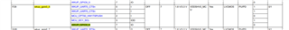
3. Identify the padconfig register address for the particular GPIO using the datasheet from section 6.4 Pin Multiplexing. Eg. PADCONFIG 50 for ballnumber F29
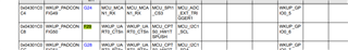
4. Identify the Kick register from the padconfig register address obtained above TRM section 5.1 Control Module Eg. padconfig 50 = 0x4301C0C8 (offset 1C0C8) so select LOCK7_KICK0 register address
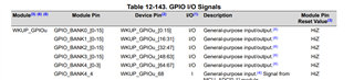
5. Identify the GPIO Bank from the GPIO number from TRM Section 12.1.2 GPIO Eg. For WKUP_GPIO0_6 it would be GPIO_BANK0
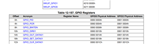
6. Get the DIR and OUT_DATA register offset w.r.t the gpio bank selected For eg. 0x42110010 GPIO_DIR01 (Includes 16bit LSB for Bank 0 and 16bit MSB for Bank 1) 0x42110014 GPIO_OUT_DATA01 (Includes 16bit LSB for Bank 0 and 16bit MSB for Bank 1)
Please find the code attached below for GPIO toggling.