Part Number: TMS320C6678
Other Parts Discussed in Thread: SYSBIOS
Hi
Please provide "DDR3 Read write test code" (or) How to do DDR3 test on C6678 EVM or K2H EVM board ?
This thread has been locked.
If you have a related question, please click the "Ask a related question" button in the top right corner. The newly created question will be automatically linked to this question.
Part Number: TMS320C6678
Other Parts Discussed in Thread: SYSBIOS
Hi
Please provide "DDR3 Read write test code" (or) How to do DDR3 test on C6678 EVM or K2H EVM board ?
"DDR3 Read write test code" (or) How to do DDR3 test on C6678 EVM or K2H EVM board ?
Pre-requisite :
1. Download and install BIOSLINUXMCSDK-K2 — MCSDK supporting SYS/BIOS RTOS and Linux OS for KeyStone II ARM A15 + DSP C66x
Version : MCSDK 3_01_04_07 from http://software-dl.ti.com/sdoemb/sdoemb_public_sw/mcsdk/latest/index_FDS.html
( Please install the SDK in the recommended path: C:\ti\)
2. Download and install CCS 9.3 , https://www.ti.com/tool/download/CCSTUDIO/9.3.0.00012
( Please install in the recommended path: C:\ti\)
3. DDR3 Project collateral and source code discussed can be downloaded from http://www.ti.com/lit/zip/sprac04
4. Once you unzip the sprac04.zip, the folder, "keystone2-ddr3-debug-tools" contains the DDR3_EDMA_TEST source code. ( or)
download directly form here: DDR3_EDMA_TEST.zip
Steps :
=======
The same steps are given in the video below:-
1. In CCS 9.3, import the project of DR3_EDMA_TEST
2. In the project properties, set the path of the PDK_LOC variable as "C:\ti\pdk_keystone2_3_01_04_07\packages"
3. In main.c, line no: 47, change the k2k to k2h like below
#include "ti/csl/device/k2k/src/cslr_device.h" // needed for Kepler specific memory map definition
#include "ti/csl/device/k2h/src/cslr_device.h" // needed for Hawking specific memory map definition
4. In the CCS project properties--> C6000 Linker -->File search path --> , include the CSL library :"ti.csl.ae66" located at /ti/csl/lib/k2h/c66/
In the C6000 compiler --> Advanced options--> predefined symbols pre-define name--->SOC_C6678
4. Build and run
5. Test it on C6678 EVM or K2H EVM
a) DIP Switch settings on "No boot mode"
b) Launch the target configuration file and connect target. This will run the gel file.
c) Load the binary of DR3_EDMA_TEST and run/execute the program
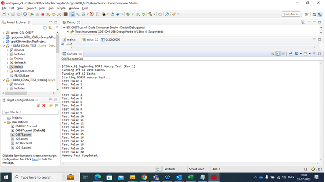
d) Observe the output as below.

The same steps are given in the video below:-
=======
For K2H:
=======
Follow the same procedure. In the pre-defined symbol, set SOC_K2H and build
DDR3 test code:
/******************************************************************************
 * Copyright (C) 2015 Texas Instruments Incorporated - http://www.ti.com/
 *
 *
 * Redistribution and use in source and binary forms, with or without
 * modification, are permitted provided that the following conditions
 * are met:
 *
 * * Redistributions of source code must retain the above copyright
 * notice, this list of conditions and the following disclaimer.
 *
 * * Redistributions in binary form must reproduce the above copyright
 * notice, this list of conditions and the following disclaimer in the
 * documentation and/or other materials provided with the
 * distribution.
 *
 * * Neither the name of Texas Instruments Incorporated nor the names of
 * its contributors may be used to endorse or promote products derived
 * from this software without specific prior written permission.
 *
 * THIS SOFTWARE IS PROVIDED BY THE COPYRIGHT HOLDERS AND CONTRIBUTORS
 * "AS IS" AND ANY EXPRESS OR IMPLIED WARRANTIES, INCLUDING, BUT NOT
 * LIMITED TO, THE IMPLIED WARRANTIES OF MERCHANTABILITY AND FITNESS FOR
 * A PARTICULAR PURPOSE ARE DISCLAIMED. IN NO EVENT SHALL THE COPYRIGHT
 * OWNER OR CONTRIBUTORS BE LIABLE FOR ANY DIRECT, INDIRECT, INCIDENTAL,
 * SPECIAL, EXEMPLARY, OR CONSEQUENTIAL DAMAGES (INCLUDING, BUT NOT
 * LIMITED TO, PROCUREMENT OF SUBSTITUTE GOODS OR SERVICES; LOSS OF USE,
 * DATA, OR PROFITS; OR BUSINESS INTERRUPTION) HOWEVER CAUSED AND ON ANY
 * THEORY OF LIABILITY, WHETHER IN CONTRACT, STRICT LIABILITY, OR TORT
 * (INCLUDING NEGLIGENCE OR OTHERWISE) ARISING IN ANY WAY OUT OF THE USE
 * OF THIS SOFTWARE, EVEN IF ADVISED OF THE POSSIBILITY OF SUCH DAMAGE.
 *
 ******************************************************************************
 *
 *	DDR3 EDMA Test
 *
 *	DDR3 Stress Test for K2 Devices
 *
 *	Revision v1.0, August 2015
 */

// Project Includes ---------------------
#include <stdio.h>
#include <stdint.h>
#include <c6x.h>
#include "ti/csl/csl.h"							// needed for CSL data type definitions
#include "ti/csl/device/k2h/src/cslr_device.h" 	// needed for Hawking specific memory map definition
#include "ti/csl/csl_cacheAux.h"				// needed for cache disable functions
#include "defines.h"

// Project Defines (User Configurable)---
#define EDMA_ON_WRITE1	1
#define EDMA_ON_WRITE2	1

#define EDMA_ON_READ1	1
#define EDMA_ON_READ2	1

#define DDR3A_TEST		1	//Select either DDR3A OR DDR3B, not both
#define DDR3B_TEST		0	//Select either DDR3A OR DDR3B, not both


// Global Declarations/Definitions ------
unsigned int test_revision = 1;

unsigned int errcnt;
unsigned int global_count;
unsigned int read_val, error_check;
unsigned int delay = 2;
unsigned int delay2 = 2000;
unsigned int delay3a = 50000;

#define L2_C66x0_GLOBAL_ADDR			(0x10800000)
#define L2_C66x0_GLOBAL_ADDR_2			(0x10808000)
#define MSMC_MEM_ADDR					(0x0c000000)
#define MSMC_MEM_ADDR_2					(0x0c010000)
#define MSMC_MEM_ADDR_3					(0x0c010000)
#define DDR3B_PHYS_ADDR					(0x60000000)

unsigned int temp_val;
unsigned int L1_cache_value;
unsigned int L2_cache_value;


/************************************************************************************
 *
 * DDR3 MPAX Configuration
 * This function configures the c66x MPAX to point the local address 0x8000_0000
 * to the upper bits of the physical address given by address_start
 *
 -----------------------------------------------------------------------------------*/
void ddr3_mpax_segment2_setup(unsigned int address_start){
	XMPAX2_L = address_start | 0x3F;	// Upper Bits of 36-bit address space
	XMPAX2_H = 0x8000001E;				//Local address of 0x8000_0000
}

void delay_func(unsigned int delay)
{
	unsigned int i;
	for(i=0;i<delay;i++);
}

/************************************************************************************
 *
 * DDR3A EDMA Config
 * This function configures the QDMA in the EDMA for burst access. The physical address
 * of the source/destination, and the size of the transfer block are given in the
 * function parameters.
 *
 -----------------------------------------------------------------------------------*/
void ddr3_edma_config(unsigned int src, unsigned int dst, unsigned int nbytes)
{
	unsigned int acnt = nbytes;
	unsigned int bcnt = 1;
	unsigned int ccnt = 1;

	// Clear the pending interrupt
	EDMA_ICR = 0x1;

	// QDMA channel 0 uses parameter set 0, trigger word 7
	EDMA_QCHMAP0 = 0x1C;

	// Enable QDMA channel 0 */
	EDMA_QEESR = 0x1;

	// PARAM 0, opt - tciintn, static and syncdim set
	EDMA_PARAM_0_0 = 0x0010000c;

	// PARAM 1 - source address
	EDMA_PARAM_0_1 = src;

	// PARAM 2 - bcount, acount
	EDMA_PARAM_0_2 = (bcnt << 16) | acnt;

	// PARAM 3, destination
	EDMA_PARAM_0_3 = dst;

	// PARAM 4  dstbidx, srcbidx
	EDMA_PARAM_0_4 = acnt;

	// PARAM 5 - link
	EDMA_PARAM_0_5 = 0xffff;

	// PARAM 6 - dstcidx, srccidx
	EDMA_PARAM_0_6 = 0;

	// PARAM 7 - ccnt
	EDMA_PARAM_0_7 = ccnt;

	// Wait until complete interrupt
	while ((EDMA_IPR & 0x1) != 1){
			delay_func(10);
		}

	// Scrub Interrupt
	EDMA_ICR = 0x1;

	// Disable QDMA Channel 0
	//EDMA_QEECR = 0x1

	// Clear the channel map
	EDMA_QCHMAP0 = 0x0;

}

/************************************************************************************
 *
 * MSM Populate Function
 * This function serves to populate the MSM of pattern and size given in the function
 * parameters. The data patterns themselves are provided in the defines.h
 * project file.
 *
 -----------------------------------------------------------------------------------*/
void populate_MSM(unsigned long long int DATA_PATTERN, unsigned int nbytes)
{
	unsigned int i;

	// Place First Data Pattern in MSM
	if (DATA_PATTERN == 1){
		for(i=0;i<nbytes;i++){
				(*(unsigned long long int*)(MSMC_MEM_ADDR+(i*0x08))) = DATA_PATTERN_inc[i];
		}
	}
	// Place Second Data Pattern in MSM
	if (DATA_PATTERN == 2){
			for(i=0;i<nbytes;i++){
					(*(unsigned long long int*)(MSMC_MEM_ADDR+(i*0x08))) = DATA_PATTERN_zeroes[i];
			}
		}
}

/************************************************************************************
 *
 * DDR3 Write Read Memory Test
 * This function serves to execute the test write->read, write->read cycles
 *
 -----------------------------------------------------------------------------------*/
void ddr3a_edma_memory_test(unsigned int DDR3_TEST_START, unsigned int nbytes)
{
	unsigned int PATTERN1 = 1;
	unsigned int PATTERN2 = 2;

	unsigned int TEST_WORDS = 2048;
	unsigned int TEST_READS = 2;
	unsigned int ERROR_MAX = 500;

	unsigned int i,j,k,errCnt=0;
	unsigned long long int doubletemp_val;

	// First pass
	// Populate MSM with 256 word pattern
	populate_MSM(PATTERN1, nbytes);
	errCnt = 0;
	for(i=0;i<TEST_WORDS;i++){
	// Block Write MSM->DDR
#if (EDMA_ON_WRITE1)
		ddr3_edma_config(MSMC_MEM_ADDR, (DDR3_TEST_START+(i*nbytes*8)), nbytes*8);

#else
		for(k=0;k<(nbytes);k++){
			(*(unsigned long long int*)(DDR3_TEST_START+(i*nbytes*8)+(8*k))) = DATA_PATTERN_inc[k];
		}
#endif

	}
#if(EDMA_ON_READ1)
	//Iterate through addresses range for read
	for(i=0;i<TEST_WORDS;i++){
		for(j=0;j<TEST_READS;j++){
			// Block Read DDR->MSM
			ddr3_edma_config((DDR3_TEST_START+(i*nbytes*8)), MSMC_MEM_ADDR_2, nbytes*8);
			// Iterate through MSM, make data comparison
			for(k=0;k<(nbytes);k++){
				doubletemp_val = (*(unsigned long long int*)(MSMC_MEM_ADDR_2 + (8*k)));
				if ((doubletemp_val != DATA_PATTERN_inc[k]) && (errCnt < ERROR_MAX)){
					printf("DMA1 Read Error @ %x, read cycle %d. Expected: %.16llx, Got: %.16llx\n",(DDR3_TEST_START+(i*nbytes)+(8*k)), j, DATA_PATTERN_inc[k], doubletemp_val);
					errCnt++;
				}
			}
		}
	}
#else
	for(i=0;i<TEST_WORDS;i++){
		for(j=0;j<TEST_READS;j++){
			for(k=0;k<nbytes;k++){
				*(unsigned long long int*)(MSMC_MEM_ADDR_3+(8*k)) = (*(unsigned long long int*)(DDR3_TEST_START+(i*nbytes*8)+(8*k)));
			}
			for(k=0;k<(nbytes);k++){
				doubletemp_val = (*(unsigned long long int*)(MSMC_MEM_ADDR_3+(8*k)));
				if ((doubletemp_val != DATA_PATTERN_inc[k]) && (errCnt < ERROR_MAX)){
					printf("Read1 Error @ %x, read cycle %d, word %d. Expected: %.16llx, Got: %.16llx\n",(DDR3_TEST_START+(i*nbytes*8)+(8*k)), j,k, DATA_PATTERN_inc[k], doubletemp_val);
					errCnt++;
				}
			}
		}
	}
#endif

	// Populate MSM with 256 word pattern
	populate_MSM(PATTERN2, nbytes);
	errCnt = 0;
	for(i=0;i<TEST_WORDS;i++){
	// Block Write MSM->DDR
#if (EDMA_ON_WRITE2)
		ddr3_edma_config(MSMC_MEM_ADDR, (DDR3_TEST_START+(i*nbytes*8)), nbytes*8);
#else
		for(k=0;k<(nbytes);k++){
			(*(unsigned long long int*)(DDR3_TEST_START+(i*nbytes*8)+(8*k))) = DATA_PATTERN_zeroes[k];
		}
#endif

	}
#if(EDMA_ON_READ1)
	//Iterate through addresses range for read
	for(i=0;i<TEST_WORDS;i++){
		for(j=0;j<TEST_READS;j++){
			// Block Read DDR->MSM
			ddr3_edma_config((DDR3_TEST_START+(i*nbytes*8)), MSMC_MEM_ADDR_2, nbytes*8);
			// Iterate through MSM, make data comparison
			for(k=0;k<(nbytes);k++){
				doubletemp_val = (*(unsigned long long int*)(MSMC_MEM_ADDR_2 + (8*k)));
				if ((doubletemp_val != DATA_PATTERN_zeroes[k]) && (errCnt < ERROR_MAX)){
					printf("DMA2 Read Error @ %x, read cycle %d. Expected: %.16llx, Got: %.16llx\n",(DDR3_TEST_START+(i*nbytes*8)+(8*k)), j, DATA_PATTERN_zeroes[k], doubletemp_val);
					errCnt++;
				}
			}
		}
	}

#else
	for(i=0;i<TEST_WORDS;i++){
		for(j=0;j<TEST_READS;j++){
			for(k=0;k<nbytes;k++){
				*(unsigned long long int*)(MSMC_MEM_ADDR_3+(8*k)) = (*(unsigned long long int*)(DDR3_TEST_START+(i*nbytes*8)+(8*k)));
			}
			// Only check first burst (assumes nbytes=256)
			for(k=0;k<(nbytes);k++){
				doubletemp_val = (*(unsigned long long int*)(MSMC_MEM_ADDR_3+(8*k)));
				if ((doubletemp_val != DATA_PATTERN_zeroes[k]) && (errCnt < ERROR_MAX)){
					//GPIO_assert();
					printf("Read2 Error @ %x, read cycle %d, word %d. Expected: %.16llx, Got: %.16llx\n",(DDR3_TEST_START+(i*nbytes*8)+(8*k)), j,k, DATA_PATTERN_zeroes[k], doubletemp_val);
					errCnt++;
				}
			}
		}
	}
#endif
	if(errCnt >= ERROR_MAX){printf("Error count hit maximum. Not all errors displayed.\n");}

	// Error Conclusion
	if(errCnt >= 1){
		printf("Error(s) found in Test iteration.\n");
	}
}

void ddr3b_edma_memory_test(unsigned int DDR3_TEST_START, unsigned int nbytes)
{
	unsigned int PATTERN1 = 1;
	unsigned int PATTERN2 = 2;

	unsigned int TEST_WORDS = 2048;
	unsigned int TEST_READS = 2;
	unsigned int ERROR_MAX = 5000;

	unsigned int i,j,k,errCnt=0;
	unsigned long long int doubletemp_val;

	// First pass
	// Populate MSM with 256 word pattern
	populate_MSM(PATTERN1, nbytes);
	errCnt = 0;
	for(i=0;i<TEST_WORDS;i++){
	// Block Write MSM->DDR
#if (EDMA_ON_WRITE1)
		ddr3_edma_config(MSMC_MEM_ADDR, (DDR3B_PHYS_ADDR+(i*nbytes*8)), nbytes*8);
#else
		for(k=0;k<(nbytes);k++){
			(*(unsigned long long int*)(DDR3_TEST_START+(i*nbytes*8)+(8*k))) = DATA_PATTERN_inc[k];
		}
#endif
	}
#if(EDMA_ON_READ1)
	//Iterate through addresses range for read
	for(i=0;i<TEST_WORDS;i++){
		for(j=0;j<TEST_READS;j++){
			// Block Read DDR->MSM
			ddr3_edma_config((DDR3B_PHYS_ADDR+(i*nbytes*8)), MSMC_MEM_ADDR_2, nbytes*8);
			// Iterate through MSM, make data comparison
			for(k=0;k<(nbytes);k++){
				doubletemp_val = (*(unsigned long long int*)(MSMC_MEM_ADDR_2 + (8*k)));
				if ((doubletemp_val != DATA_PATTERN_inc[k]) && (errCnt < ERROR_MAX)){
					printf("DMA1 Read Error @ %x, read cycle %d. Expected: %.16llx, Got: %.16llx\n",(DDR3_TEST_START+(i*nbytes*8)+(8*k)), j, DATA_PATTERN_inc[k], doubletemp_val);
					errCnt++;
				}
			}
		}
	}
#else
	//Iterate through addresses range for read
	for(i=0;i<TEST_WORDS;i++){
		for(j=0;j<TEST_READS;j++){
			// Read DDR->MSM
			for(k=0;k<nbytes;k++){
				*(unsigned long long int*)(MSMC_MEM_ADDR_3+(8*k)) = (*(unsigned long long int*)(DDR3_TEST_START+(i*nbytes*8)+(8*k)));
			}
			// Iterate through MSM, make data comparison
			for(k=0;k<(nbytes);k++){
				doubletemp_val = (*(unsigned long long int*)(MSMC_MEM_ADDR_3+(8*k)));
				if ((doubletemp_val != DATA_PATTERN_inc[k]) && (errCnt < ERROR_MAX)){
					printf("Read1 Error @ %x, read cycle %d, word %d. Expected: %.16llx, Got: %.16llx\n",(DDR3_TEST_START+(i*nbytes*8)+(8*k)), j,k, DATA_PATTERN_inc[k], doubletemp_val);
					errCnt++;
				}
			}
		}
	}
#endif


	// Second Pass
	// Populate MSM with 256 word pattern
	populate_MSM(PATTERN2, nbytes);
	errCnt = 0;
	for(i=0;i<TEST_WORDS;i++){
	// Block Write MSM->DDR
#if (EDMA_ON_WRITE2)
		ddr3_edma_config(MSMC_MEM_ADDR, (DDR3B_PHYS_ADDR+(i*nbytes*8)), nbytes*8);
#else
		for(k=0;k<(nbytes);k++){
			(*(unsigned long long int*)(DDR3_TEST_START+(i*nbytes)+(8*k))) = DATA_PATTERN_zeroes[k];
		}
#endif

	}
#if(EDMA_ON_READ2)
	//Iterate through addresses range for read
	for(i=0;i<TEST_WORDS;i++){
		for(j=0;j<TEST_READS;j++){
			// Block Read DDR->MSM
			ddr3_edma_config((DDR3B_PHYS_ADDR+(i*nbytes*8)), MSMC_MEM_ADDR_2, nbytes*8);
			// Iterate through MSM, make data comparison
			for(k=0;k<(nbytes);k++){
				doubletemp_val = (*(unsigned long long int*)(MSMC_MEM_ADDR_2 + (8*k)));
				if ((doubletemp_val != DATA_PATTERN_zeroes[k]) && (errCnt < ERROR_MAX)){
					printf("DMA2 Read Error @ %x, read cycle %d. Expected: %.16llx, Got: %.16llx\n",(DDR3_TEST_START+(i*nbytes*8)+(8*k)), j, DATA_PATTERN_zeroes[k], doubletemp_val);
					errCnt++;
				}
			}
		}
	}

#else
	//Iterate through addresses range for read
	for(i=0;i<TEST_WORDS;i++){
		for(j=0;j<TEST_READS;j++){
			// Read DDR->MSM
			for(k=0;k<nbytes;k++){
				*(unsigned long long int*)(MSMC_MEM_ADDR_3+(8*k)) = (*(unsigned long long int*)(DDR3_TEST_START+(i*nbytes*8)+(8*k)));
			}
			// Iterate through MSM, make data comparison
			for(k=0;k<(nbytes);k++){
				doubletemp_val = (*(unsigned long long int*)(MSMC_MEM_ADDR_3+(8*k)));
				if ((doubletemp_val != DATA_PATTERN_zeroes[k]) && (errCnt < ERROR_MAX)){
					//GPIO_assert();
					printf("Read2 Error @ %x, read cycle %d, word %d. Expected: %.16llx, Got: %.16llx\n",(DDR3_TEST_START+(i*nbytes*8)+(8*k)), j,k, DATA_PATTERN_zeroes[k], doubletemp_val);
					errCnt++;
				}
			}
		}
	}
#endif
	if(errCnt >= ERROR_MAX){printf("Error count hit maximum. Not all errors displayed.\n");}

	// Error Conclusion
	if(errCnt >= 1){
		printf("Error(s) found in Test iteration.\n");
	}
}

void main(void) {

	unsigned int counter=0;

	printf("Beginning DDR3 Memory Test (Rev %d)\n", test_revision);

	printf("Turning off L1 Data Cache.\n");
	CACHE_setL1DSize(CACHE_L1_0KCACHE);
	printf("Turning off L2 Cache.\n");
	CACHE_setL2Size(CACHE_0KCACHE);

#if(DDR3A_TEST)
		printf("Starting DDR3A memory test...\n");
#elif(DDR3B_TEST)
		printf("Starting DDR3B memory test...\n");
#endif

	while(counter < 500){
#if(DDR3A_TEST)
		ddr3a_edma_memory_test(0x80000000, 256);
#elif(DDR3B_TEST)
		ddr3_mpax_segment2_setup(0x08000000);
		ddr3b_edma_memory_test(0x80000000, 256);
		ddr3_mpax_segment2_setup(0x80000000);
#endif
		counter++;
		if((counter % 25) == 0){
			printf("Test Pulse %d\n", counter/25);
		}
	}


	printf("Memory Test Completed.\n");

}
Visit these FAQs on "How to calculate the "DDR3 Interface – Registers" for Keystone devices and Test/Debug on Keystone EVM"
Keystone - I
Keystone - II
Regards
Shankari G
HI all,
Changes required to run the sample DDR3 test code using processor SDK 6.3
========================================================
If you are using the latest software package - processor SDK 6.3, for example:- "PROCESSOR-SDK-RTOS-K2HK 06_03_00_106
https://software-dl.ti.com/processor-sdk-rtos/esd/K2HK/latest/index_FDS.html"
please do the following changes.
-------------------------------------------
1. In the project properties, set the path of the PDK_LOC variable as "C:\ti\pdk_k2hk_4_0_16\packages"
2. In main.c, line no: 47, change the path like below
#include "ti/csl/cslr_device.h"
3. In the CCS project properties--> C6000 Linker -->File search path --> , include the CSL library :"ti.csl.ae66" located at C:\ti\pdk_k2hk_4_0_16\packages\ti\csl\lib\k2h\c66\release\ti.csl.ae66
All the other steps are same as above.
Regards
Shankari G
Hi all,
If interested to do throughput measurement for the DDR3 read / write test, please do the following changes in the main.c
====
Steps:-
=====
1. Include the header file of "TSC" - Time stamp counter. We are going to use two functions, " CSL_Uint64 CSL_tscRead (void)" and "void CSL_tscEnable(void)" for this experiment.
#include <ti/csl/csl_tsc.h>
2. Declare the TSC registers as "extern"
/*****************************************************************************
* Function: Utility function a cycle clock
****************************************************************************/
extern cregister volatile unsigned int TSCL;
extern cregister volatile unsigned int TSCH;
3. In main() function, initialize the variables and the TSC registers used to calculate the time period.
void main(void) {
/*Throughput calculation initialization */
CSL_Uint64 StartTime = 0;
CSL_Uint64 EndTime = 0;
CSL_Uint64 Total_cycle_ticks = 0;
/*Throughput calculation initialization Ends */
unsigned int counter=0;
/* Enable the time stamp counter. */
CSL_tscEnable();
TSCH = 0;
TSCL = 0;
4. Call the tsc read functions at appropriate places like below.
#if(DDR3A_TEST)
printf("Starting DDR3A memory test...\n");
#endif
StartTime = CSL_tscRead();
while(counter < 4){
#if(DDR3A_TEST)
ddr3a_edma_memory_test(0x80000000, 256);
#endif
counter++;
}
EndTime = CSL_tscRead();
Total_cycle_ticks = EndTime-StartTime;
printf("StartTime = %llu \n", StartTime);
printf("EndTime = %llu \n", EndTime);
printf("Total_cycle_ticks = %llu \n", Total_cycle_ticks);
printf("Memory Test Completed.\n");
}
Test results:
=========
This testing includes the read, write and verify. ( Read was done in 2 iterations / Two patterns of data are written)
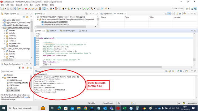
--- > Using MCSDK 3.01 , it takes 2.95 seconds.
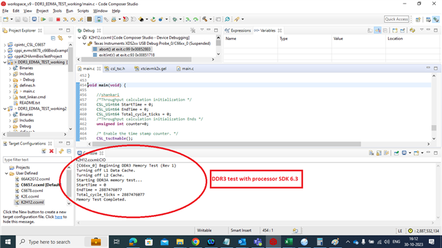
----> Using processor SDK, it takes 2.93 seconds.
==============
Test set up details:
==============
1. DDR3 is driven only by DSP core.
2. DSP core frequency is 983 MHz.
3. DDR3 clock frequency is 666 MHz.
4. The CSL package of MCSDK 3.01 is used for first test.
5. The CSL package of processor SDK is used for the second test.
6. Please note, No Operating System ( SYSBIOS/ RTOS) is used. This is just a baremetal code with CSL header files.
===================
Test 1 with MCSDK 3.01:-
===================

MCSDK - Clock calculation with respect to the core frequency.
------------------------------------------------------------------
Total no of CPU cycles = 2900268968 cycles
DSP core frequency = 983 MHz
Time = 1 / Freq ( General formula )
= 1 / 983 MHz ( DSP core frequency )
= 0.001017 us ( Micro seconds)
983000000 cycles = 1 sec
=>2900268968 cycles = 2.95 seconds
===================
Test 2 with processor SDK 6.3 :-
===================

Processor SDK - Clock cycle calculation with respect to the core frequency.
------------------------------------------------------------------
Total no of CPU cycles = 2887476077 cycles
DSP core frequency = 983 MHz
Time = 1 / Freq ( General formula )
= 1 / 983 MHz ( DSP core frequency )
= 0.001017 us ( Micro seconds)
983000000 cycles = 1 sec
=>2887476077 cycles = 2.93 seconds
----
Regards
Shankari G