Hi, Clemens,
Further information in the similiar part SN74CB3T3257 detail the Vgate=VCC+VT , should be a charge bump inside?
Best Regards,
James
A closed switch behaves like a small resistor; the voltage between the S/D pins is noticeably different only if a large current flows.
If you cannot use the SN74CB3T3257, you need an actual level shifter.
Part Number: SN74CB3T3245
9.2.3 Application curves: I think the Io parameter is wrong: Io = 1 mA should be 1 uA...
Compare e g the corresponding diagram in scda008, 5.3.1.1 (figure 30); sn74cb3t3257 Figure 3; sn74cb3t16210 Figure 3
Part Number: SN3257-Q1
Hi,
We are looking at using SN3257-Q1 as a multiplexer and voltage level shifter. The input is from a microprocessor (TMS570) and a seperate hardware safety circuit (for FUSA) - the mux logic is used to determine which input line is passed through to a UCC21710 gate driver. The input parts operate at 3,3V whereas the gate driver is on a 5V rail.
In our design the input signals are 0-3,3V (low-high logic) - the outputs are to the gate driver UCC21710 which requires (we believe 5V input on the gate drive signal live - datasheet shows minimum of 70% of VCC (ie. 0.7x5V = 3,5V).
Is there a design adjustment we can use to satisfactorily lift the input signal from 3,3V all the way to 5V or at least adequate to robustly drive the IN+ line on the gate driver.
In all respects we were very attracted to SN3257-Q1 as the datasheet implied that a 1.8V input could be output at 3,3V however we are not clear on this now.
Thanks,
John
Hi Krishnamoorthy,
The connection of two cameras with only one in use simplifies the muxing but you need to know if the camera is generating the VD, HD and C_FIELD signals. If these signals are provided by the camera a set of buffers with tri-state outputs would allow one or the other camera to drive the camera interface. If those signals are inputs to the camera you will have a buffer and drive them to both cameras. The delay through the buffer would have to be considered when analyzing the timing. The other possible method would be to use a low voltage FET multiplexer such as the SN74CB3T3257 to switch between the two camera interface. These are bidirectional switches so the direction of the VD, HD and C_FIELD signals could be either input or output.
Regards, Bill
Hello!
I need a few signal switches, but I cannot figure out whether to use digital multiplexers or analog switches.
I need a couple of quad 2:1 muxes, a couple of single channel 2:1 muxes and a single 9:1 mux, which could be splitted in 8:1 + 2:1.
The worst case signals I have to pass are 8 MHz clocks, and my main task is to have the smallest possible input-output propagation delay (selection-output propagation delay does not matter). I found some parts (mainly SN74CBTLV3251 and SN74CB3T3257), but I am not sure if they are the right parts for me. And I don't understand why on the analog switches' data sheets there is no mention of input-output propagation delays.
Can you please help?
Thanks in advance.
Stefano Infante
Hi Anne,

I recommend using TMUX1574 compared to the other SN74 devices you mentioned. Check out the s-parameter model for TMUX1574 to simulate measurements, such as bandwidth, for this application!
Regards,
Kate
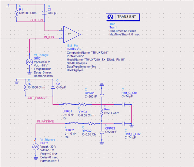
Many of TI’s analog switches and multiplexers have an associated IBIS model with them. However not every analog switch and multiplexer has an IBIS model and sometimes the IBIS model does not include the switch pathway characteristics. However, since an analog switch’s/multiplexer’s through path is not very complicated a simplified passive stand in model can be used. This FAQ will walk through what the passive model will look like, what to do when there is a partial IBIS model, what to do when there is no IBIS model, and finally a comparison between a full IBIS model and the simple passive model using ADS.
Passive Approximation of Analog Switch/Multiplexer IBIS Model
The passive model is shown below:
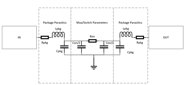
The switch is broken into three pieces. The first is package parasitics – this is the inherent RLC values that are associated with the lead into the switch. This is defined in the IBIS file for both full and partial IBIS models. The middle section is data from the datasheet on the switch parameters about on resistance and on capacitance. These values can be used to approximate the switch pathway when it is closed. Finally, the last section is package parasitics – which is identical to the first block. For a typical room temperature simulation, the typical values should be used on both package and switch, while max temperature can be approximated with max values for both package and switch.
Only Partial IBIS Model Available – No Through Path Data
If the IBIS model available does not contain through path data the passive model can be used. For this example, take the TMUX1119 which currently as of December 2021 only has a partial IBIS model. To create a passive stand-in, choose the package for the TMUX1119, let’s use the DCK package. To create the passive model first open the TMUX1119 IBIS model and look at the package data for the TMUX1119DCK.
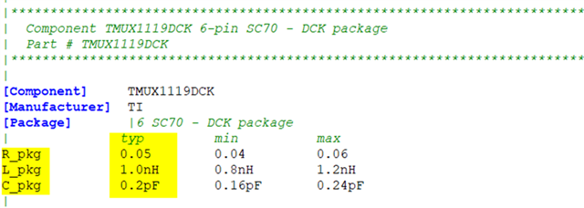
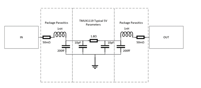
The typical package parameters are highlighted – this takes care of the first and last block of the passive model with Rpkg = 50mΩ; Lpkg = 1nH; Cpkg = 200fF. This is for the typical case – if max temperature simulation uses the max values from the package data should be used.
Next the switch parameters need to be taken – let’s assume that we are operating this simulation at 5V. Since the simulation is at 5V we need the typical on resistance and typical on capacitance from the datasheet.
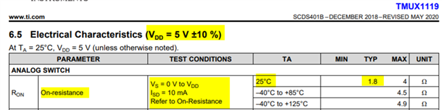

With the typical conditions for the switch, on resistance can be set to 1.8Ω and on capacitance is 20pF where half of that value is 10pF. Now the passive model at 5V can be put together.
Only Partial IBIS Model Available – Missing Package Data
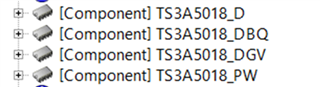
Sometimes a model exists – but the package that is desired does not exist. By editing the IBIS model, a new package can be added from a similar existing package. To show how this is done the TS3A5018 in the RSV package. The current TS3A5018 has the following packages:
The package header is structured quite simply however:
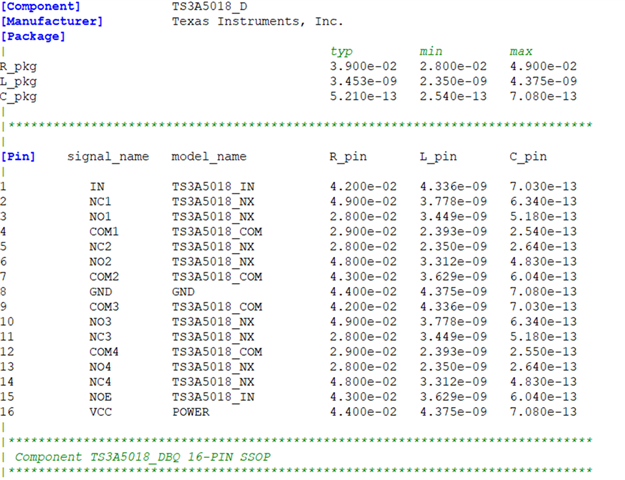
To get the RSV package data – a part with the same package should be chosen. For this example, the TMUX1111RSV will be used – this data is shown below:
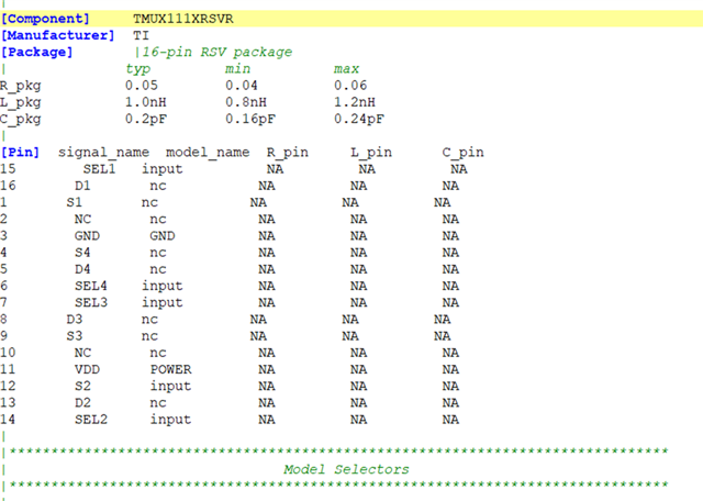
Please note that it is generally uncommon for every pin to be defined in the multiplexer or switch IBIS models – so if the package is defined it should be okay.
First this text from the TMUX1111 needs to be changed to match the TS3A5018.
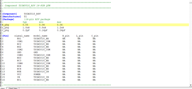
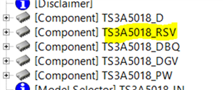
And now a full featured IBIS model of the TS3A5018RSVR is available for simulation.
No IBIS Model Available
Not all of TI’s switches/multiplexers have an IBIS model. While grabbing the switch parameters is the same as in the partial model – what about package parameters? To approximate these values, search for an IBIS model with the same or similar package – as the parameters should be very similar. To demonstrate how to build a model without a partial model to start with, the TMUX1574 in the PW package at a 3.3V supply will be used (no IBIS model for the TMUX1574 as of 12/14/2021). This is a 16 pin PW (TSSOP) package – so the first step is to find other multiplexers from TI in the same or similar package. To do this use the parameter search table and enter the configuration and channel count of the switch, and then filter based on package group. For the TMUX1574, a 4 channel 2:1, there are multiple options – but the SN74CB3T3257 is offered in the same package as the TMUX1574PWR, and while it may be slightly different it is a good approximation of the package parameters. Its IBIS package data is shown below.
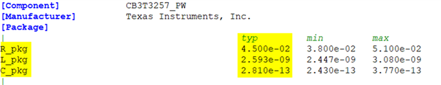
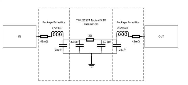
So, for the TMUX1574, a typical simulation will have Rpkg = 45mΩ; Lpkg = 2.593nH; and Cpkg = 281 fF. This takes care of the first and third block of the passive model.
Finally, the TMUX1574 model can be complete when the switch parameters are read from the datasheet. This is shown below
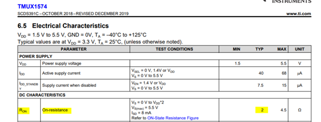

This finalizes the typical switch characteristics with an on resistance of 2Ω and an on capacitance of 7.5pF with half of that being 3.75pF. This leads us to the following passive model.
Comparison of IBIS Model Vs. Passive Stand-In
To help show the value in using a passive model when there is no available full model a simulation between a passive and full IBIS model can be shown. For this example, the TMUX7219 will be used in the DGK package at a supply voltage of +/-15V and a load of 1kΩ + 5pF. This will be compared to the passive model using the same methods as above to create the passive stand-in. The source is a 40KHz triangle wave that goes from -15V to 15V, one half period will be shown (the rise from -15V to 15V). The test was done using Advanced Design System 2021 (ADS) as the simulator and the set-up is shown below, where the top circuit is the IBIS model and the bottom is the passive stand in:
The following results are generated after the voltage sweep:
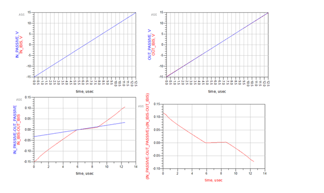
The top left graph shows the passive and IBIS models input voltage – it is the same so only one line can be seen. The top right graph shows the outputs of both models – blue for passive and red for IBIS. There is a very small difference that is best seen at the lower output voltages, as the blue line is slightly higher on the y axis, this is clear first few microseconds of the graph; however, they are very similar. Finally, the third graph shows the difference in attenuation over the sweeping voltage. The red line is the IBIS model which has its attenuation vary more with input voltage compared to the passive stand in model. However, the difference is not large as over the range -15V to 15V the difference between attenuation is small and this is shown in the bottom right hand graph. This shows the difference max for this simulation is about 12mV over this range. This is a very small voltage difference, and while it does create some error this is very close to the actual model and if a full model is not available using the passive stand in can still help is approximating system performance.
Jason,
The way to answer your question is to use the ti.com switch search tool. In order for a switch to be p2p it will need to have that same configuration and channel count.
The search tool below is filtered on configuration 2:1 and 4-channles. Next you can sort these 9 devices by on-state capacitance from least to greatest.
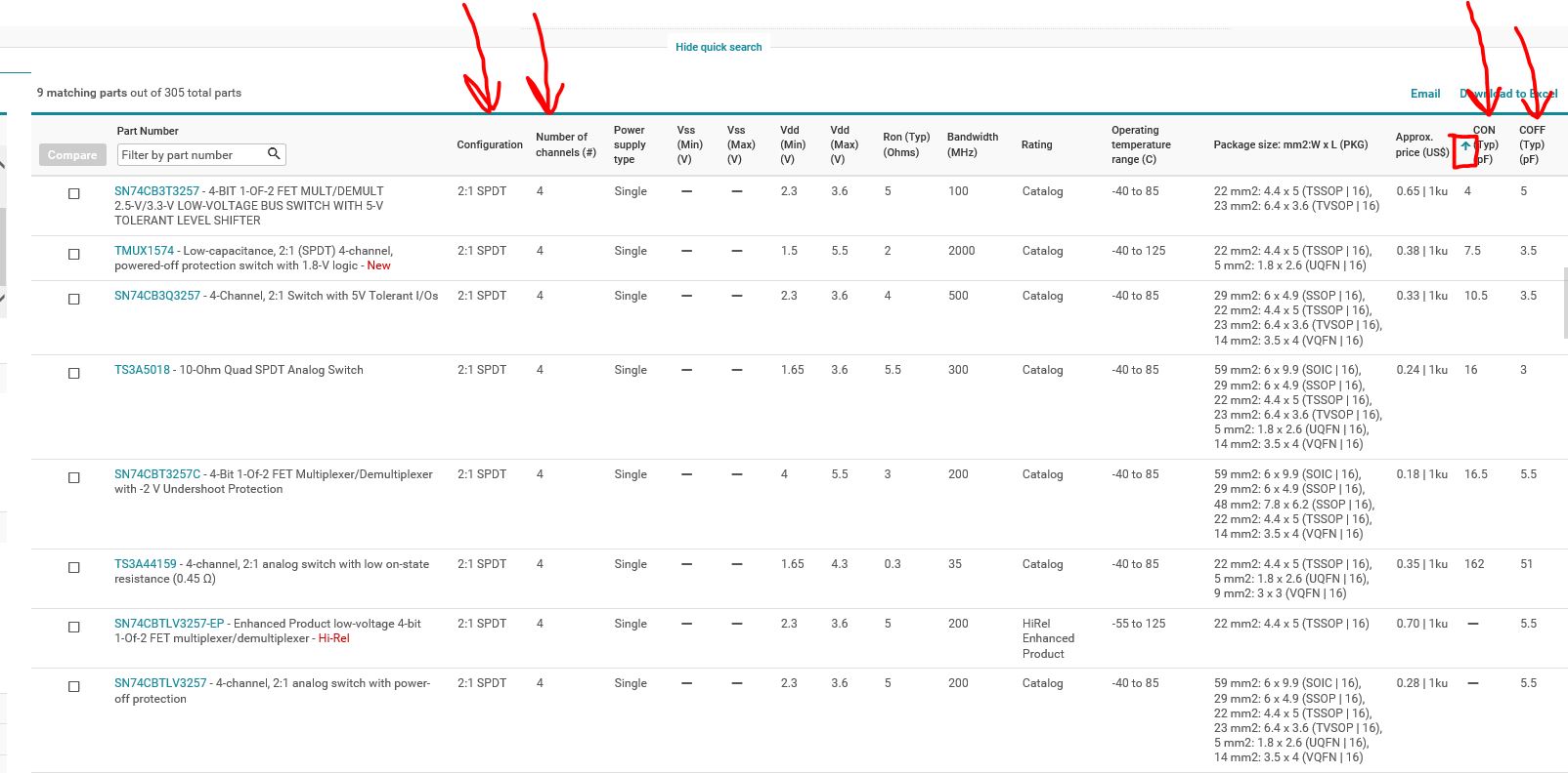
The next step is to look at the datasheets of the devices with lower on-state capacitance than the TS3A44159 and compare the pinouts. Be aware there are different names different types of pins:
power supply pins V+, Vdd, Vcc, Vss
control logic pins EN, IN, SEL, OE,
signal path COM, NO, NC, S, D

Comparing the pinouts of the lower capacitance SN74CB3T3257, TMUX1574, SN74CB3Q3257, TS3A5018, SN74CBT3257C, you can conclude that there is not a pin compatible solution for the TS3A44159.
You may notice on the table there is an inverse relationship between the on-state capacitance and on-state resistance.
What is driving the need for a lower capacitance device?