Because of the holidays, TI E2E™ design support forum responses will be delayed from Dec. 25 through Jan. 2. Thank you for your patience.

This thread has been locked.

If you have a related question, please click the "Ask a related question" button in the top right corner. The newly created question will be automatically linked to this question.

Debugging DRV8313EVM JTAG/USB

Other Parts Discussed in Thread: DRV8313EVM, ENERGIA, DRV8308EVM, MSP430G2553, DRV8313

Hi All,

I am trying to get my DRV8313EVM loaded with some custom firmware and get told no USB FET could be found in CCS when going to debug. I hooked up my MSP430 launch pad, hit debug and it worked.

This tells me CCS is configured correctly. I think either what I'm trying to do is not going to work or there is a driver issue. Energia see's the USB connection, in device manager it is listed as a "USB SERIAL PORT (COM65)" under "Ports (COM & LPT)".

The are numerous references to J4 in document SLVU815 but does not give any indication on its use (at least not to a newbie like me).

I have J2 open.

This makes me think the following

1) The USB interface is for the GUI only

2) An extra piece of hardware is required to interface with J4 and the computer.

Can somebody please confirm if those 2 points are true if so what extra part do I need to get? If I can use the USB interface with CCS, do I need an additional driver?

Thanks


Adam

  • Hi Adam,

    You are correct. The USB is for the GUI only and you do need an extra piece of hardware.

    The documentation does not mention that you will need a LaunchPad (MSP-EXP430G2) with a 4-pin header soldered to J4. This will be added to the User's Guide.

    Please see the link as an example: https://e2e.ti.com/cfs-file/__key/communityserver-discussions-components-files/38/DRV8308EVM_5F00_TEST.pdf

    This link is for the DRV8308EVM but the concepts are similar. The connections are different.

    Our apologies for the omission.

  • Hi Rick,

    Thanks again for your answer and working on a Saturday! If I could, I'd send a beer.

    I have the MSP-EXP430G2 so maybe I can do this today.

    From that are the following true:

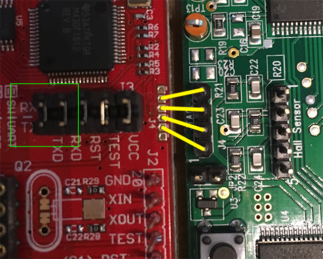
    1) I need to rotate the 2 far left (RXD/TXD) jumpers 90degrees as they are in the picture in your document (highlighted in green below)

    2) The pins connect straight across if both J4 jumpers are in parallel (highlighted in yellow below).I tried to determine from both schematics which pin connects where but couldn't quite figure this out so I have assumed that the example in your document (J4-J2) is the same for the J4-J4 on the DRV8313EVM.

    Thanks again,

    Adam

  • Hi Rick,

    After doing some extra research your comment about the connections finally clicked. I see it now looking at the schematic for DRV8308EVM and MSP-EXP430 design docs.

    I've pieced my understanding together from various sources.

    Source docs:
    www.ti.com/.../msp430g2553.pdf
    www.ti.com/.../msp-exp430g2 (slac437-1.zip/MSP-EXP430G2_Schematic+Silkscreen.pdf)
    www.ti.com/.../slvc552 (SLVC597.ZIP/schematic.pdf)

    IN 8313EVM
    Pin 1 is 3.3v
    Pin 2 is labeled TEST, which is labeled "TEST/SBWTCK" on MSP430G2553.
    Pin 3 is labeled UC_RST which is labeled "RST/NMI/SBWTDIO" on MSP430G2553.
    Pin 5 is GND

    J4 of DRV8308EVM
    PIN4=V3P3X
    PIN3=SBWTCK
    PIN2=SBWTDIO
    PIN1=GND

    MSP-EXP430G2 J2:
    Pin 2 is EZ_VCC
    Pin 3 is SBWTCK
    Pin 4 is SBWTDIO
    Pin 5 is GND

    So from this I conclude that:
    Pin 1 on 8313EVM should connect to EZ_VCC (2) on J4 of MSP-EXP430G2
    Pin 2 on 8313EVM (TEST/SBWTCK) should go to J4/Pin 3 on MSP-EXP430G2
    Pin 3 on 8313EVM (UC_RST/SBWTDIO) should go to J4/Pin 4 on MSP-EXP430G2
    Pin 4 on 8313EVM should connect to GND of J4 on MSP-EXP430G2


    I think that through various PDFs I think this is correct although most of this is done on the assumption that naming convesions are broadly similar (IE UC_RST is same as RST)

    So In my image, pin 1 on the 8313EVM (bottom pin) should go to pin 2 on the MSP (Second from top) etc.

  • Hi Adam,

    You are correct; the jumpers should be rotated as shown.

    The pins do not appear to be straight across for the DRV8313. It appears the order is reversed.

    If we use you example and number the pins on the launchpad from top to bottom as 1 through 6, the correct order is:
    Left Right
    1 Not connected
    2 1
    3 2
    4 3
    5 4
    6 Not connected

    Pins 1 to 4 of J4 on the DRV8313 are labeled from bottom to top.

    If you want to confirm this prior to making the connections , pin 5 on the launchpad and pin 4 on the DRV8313EVM should both be GND.
  • Hi Adam,

    I missed your earlier reply. Thank you for taking the time to research the connections.

    We came to the same conclusion. Have a good weekend and good luck programming.
  • HI Rick,

    Thanks again for confirming. I'm having such a blast with this as it is entirely new but still cautious so your confirmation is helpful. I wanted to try and figure something for myself and I'm glad I did, I learned a bunch from the exercise itself.

    I just hooked up the pins to the launchpad and the PWR led came on with no pop or smoke and was able to hit debug in CCS with DRV8313_Release and the debugger reloaded right up with issue so that pin configuration seems good to me.

    Thanks again for your time, have a good weekend. My weekend will now be spent trying to make my motor dance with the closed loop source.

    Adam