This thread has been locked.

If you have a related question, please click the "Ask a related question" button in the top right corner. The newly created question will be automatically linked to this question.

AM335x # of Chip Select on GPMC->EDMA data transfer

Hello,
We are debugging GPMC/EDMA data transfers on ICE3359 and facing strange phenomenon on GPMC BUS.
As the GPMC/EDMA data transfer, we transfer NOR FLASH to DDR2 by way of GPMC and EDMA.

Transfer Path: NOR FLASH -> GPMC -> EDMA -> DDR2

<GPMC/EDMA Settings>
  GPMC Settings
        -Asynchronous mode
        -16Bit Bus Size
        -Single Access
        -Using CS0 

  EDMA Settings 
     -AB Transfer
     -aCnt=2,cCnt=1 and choose number of word(16b) by setting bCnt.
        -TCINTEN=1
        -TCC=12
        -TCCMODE=0
        -STATIC=0
        -DAM=0
        -SAM=0

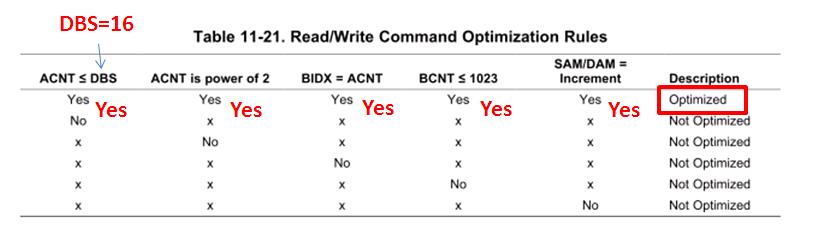
As the results, the number of GPMC Chip select signal is different from EDMA tranferred count number.
We checked the following combinations of the transfers, pls see the following table.


           Desired     Result of
 aCnt bCnt # of Words  # of Chip Select   Comments
   2    2     2          2           OK,the desired words is the same as the number of CS. 
   2    3     3          4           NG, CS should be three.
   2    4     4          4           OK,the desired words is the same as the number of CS.            
   2    7     7          8           NG, CS should be seven.
   2    9     9         16           NG, CS should be nine.
   2   12    12         16           NG, CS should be twelve.
   2   15    15         16           NG, CS should be fifteen.
   2   17    17         24           NG, CS should be seventeen.
   2   25    25         32           NG, CS should be twenty-five.

Why does not the bCnt value equal to the CS cycle?
The number of CS should be the same as bCnt value.
  
Is this a GPMC specification when we use GPMC/EDMA path?
Could you pls tell us how to accomplish the desired word transfer on GPMC/EDMA Path?

Best regards,
AY0689

  • Hello,
    we continue to debug the NOR FLASH->GPMC->EDMA->DDR2 data transfer program.

    By changing srcBIDX/dstBIDX values, the Chip Select Signal seems to be the same count as bCnt value that we set.

    At first, 16 counts of the CS are generated under aCnt=2,bCnt=9,srcBIDX=2,dstBIDX=2.

    Pls see the following results,
                                            # of CS  Result  
    1. aCnt=1,bCnt=7 ,srcBIDX=1,dstBIDX=1 =>   4      NG
    2. aCnt=1,bCnt=9 ,srcBIDX=1,dstBIDX=1 =>   8      NG
    3. aCnt=1,bCnt=13,srcBIDX=1,dstBIDX=1 =>  16      NG
    4. aCnt=1,bCnt=13,srcBIDX=1,dstBIDX=1 =>  16      NG
    -----------------------------------------------------------------
    5. aCnt=3,bCnt=4 ,srcBIDX=3,dstBIDX=3 =>  16      NG
    6. aCnt=1,bCnt=7 ,srcBIDX=2,dstBIDX=2 =>   7      OK
    7. aCnt=2,bCnt=7 ,srcBIDX=2,dstBIDX=4 =>   8      NG
    8. aCnt=2,bCnt=7 ,srcBIDX=4,dstBIDX=4 =>   7      OK
    9. aCnt=2,bCnt=15,srcBIDX=4,dstBIDX=4 =>  15      OK
    -----------------------------------------------------------------
    10. aCnt=2,bCnt=3 ,srcBIDX=4,dstBIDX=2 =>  3      OK
    11. aCnt=2,bCnt=13,srcBIDX=4,dstBIDX=2 => 13      OK
    12. aCnt=2,bCnt=15,srcBIDX=4,dstBIDX=2 => 15      OK

    When we set srcBIDX=4 and dstBIDX=2, bCnt is the same as CS numbers as the result.
    But this case is required for special source address location as the following image.
    The source data are located in the discrete address.

    It is very difficult to use.

    Could you please tell me how to set the related EDMA registers in order to transfer from Sequential Source Location to Sequental Destionation on srcBIDX=4 and dstBIDX=2 as the following image?

    Best regards,

    AY0689


  • Hello,

    this phenomenon seems to be caused by the EDMA Command Optimization Rules.
    Pls see 11.3.12.1.1   Command Fragmentation on AM335x TRM.

    I added the setting values of our transfers as follows,

    Table 11-21

    The difference between CS count and bCnt value causes by the OPTIMIZATION.
    The OPTIMAZATION sometimes changes 1 word data(16bit) to 2 byte data in the transfers.

    I showed NOR FLASH to DDR2 transfer before. In fact, the GPMC BUS is connected to FPGA.
    This FPGA has only capability of 16-bit wide access and does not have 8-bit bus access mode.

    The OPTIMIZATION may causes 8-bit access on GPMC devices.

    Could you pls tell us how to unify GPMC bus-access to the limited 16bit(Word) access under the OPTIMIZED condition?

    We need to solve this problem asap. Pls help.

    Best regards,
    AY0689

  • Greetings ay0689.

    I will start developing the same setup as yours soon. Though i will not have an answer asap be sure i will post my results.

    Hope someone from TI will answer soon...

    (Oh and i have seen similar behavior with optimized code and memcpy command to EPI(similar to gpmc for the stellaris family) didn't had the time yet to resolve that issue.) 

  • Greetings again ay0689.

    I made some tests and my setup works fine with your a_b_c Cnt combinations both in A and A_B sync mode.

    You dont mention if you have set Syncdim correctly  for the transfer mode (A/AB sync).

    i guess you have correcly linked paramsets together and you are not just one shooting transfers.

    Have you configured config1 register of gpmc for 16bit transfers ?

    Also your src-destBIDX you say are 1 ? why ? plz refer to edma low level driver document at page 16-11 

     for 3d transfer 

  • I had this same problem doing 16-bit GPMC transfers. In my case, BCNT was 10 (20 bytes) but EDMA issued 16 chip selects (32 bytes with OEn and WEn not asserted for the last 6 chip selects). Table 11-21 is the key; you need to prevent the transfer from being "optimized". I initially had BIDX=ACNT=2 but since my destination is a FIFO, I should have set "BIDX=0". Now it only issues the expected number of chip selects so we’re happy.

    Getting back to my original observation of extra chip selects due to optimized transfer. Section 11.3.12.1.1 talks about DBS (configured by tptc_cfg in Control Module, section 9.3.1.19). On my setup, the default burst size for all 3 transfer controllers was set to 3 which means 128 bytes. Based on a 16-bit transfer with ACNT=2, BCNT=10, AIDX=2, BIDX=2, SAM/DAM=INCREMENT, DBS=128, could someone explain how it decided to only do 16 chip selects since DBS is so much higher? It looks like there is another mechanism that forces the length to 32 byte chunks. I tried changing the alignment of my source and destination pointers but that had no effect. However, changing DBS to 8 (minimum setting) did eliminate the extra chip selects. It's kind of cool to watch this on a scope because you can change tptc_cfg on the fly.