Because of the Thanksgiving holiday in the U.S., TI E2E™ design support forum responses may be delayed from November 25 through December 2. Thank you for your patience.

This thread has been locked.

If you have a related question, please click the "Ask a related question" button in the top right corner. The newly created question will be automatically linked to this question.

AM335x DDR3 routing for 6 layer PCB stackup

The AM335x datasheet describes a 4 layer stackup of the minimum PCB stackup.

A 6 layer stackup is shown as follows.

LAYER TYPE DESCRIPTION
  1  Signal Top signal routing
  2  Plane Ground
  3  Plane Split Power Plane
  4  Signal Internal routing
  5  Plane Ground
  6  Signal Bottom signal routing

I understand that all of these signals should be routed first on layer 1 (Top). If it is not possible to route all of these signals on layer 1 (Top), which of layer 4 (Internal) or layer 6 (Bottom) should the remains be routed on?

Best regards,

Daisuke


  • Hi Daisuke-san,

    The Beaglebone Black is a very good example of 6-layer PCB. You can find the PCB files here: http://elinux.org/Beagleboard:BeagleBoneBlack#Hardware_Files There are Allegro, Altium and Mentor Graphics versions of the PCB.

  • Hi Biser,

    Thank you for your reply.

    Two 8-Bit DDR3 Devices are used. Is the AM335x General Purpose EVM Board a very good example of 6-layer PCB?

    processors.wiki.ti.com/.../AM335x_General_Purpose_EVM_Board_Design_Files

    Could you answer my first question? For 6-layer PCB, which of layer 4 (Internal) or layer 6 (Bottom) should the signals be routed on?

    The note of Table 7-59 on the datasheet describes:

    "All signals that have critical signal integrity requirements should be routed first on layer 1. It may not be possible to route all of these  signals on layer 1 which requires some to be routed on layer 4. When this is done, the signal routes on layer 4 should not cross splits in  the power plane."

    Best regards,

    Daisuke


  • Daisuke Maeda said:
    Two 8-Bit DDR3 Devices are used. Is the AM335x General Purpose EVM Board a very good example of 6-layer PCB?

    Yes, Rev.1.5 uses two 8-bit DDR3 memories, but I don't think the PCB file is available.

    Daisuke Maeda said:
    Could you answer my first question? For 6-layer PCB, which of layer 4 (Internal) or layer 6 (Bottom) should the signals be routed on?

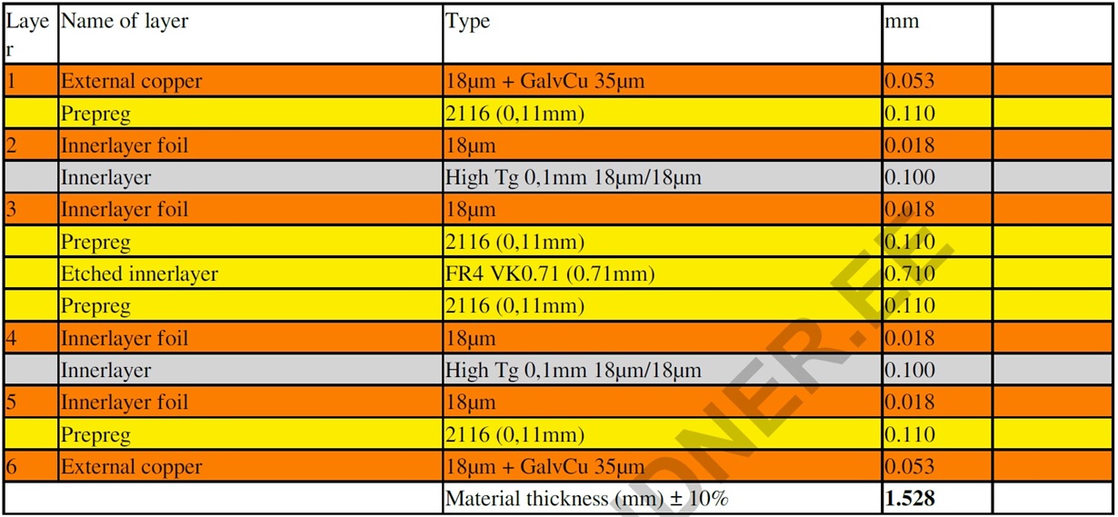
    You can use any layer that's referenced to a power/ground plane layer, so that 50Ohm single-ended and 100Ohm differential trace impedance is achieved. The note you mention should also be observed. The Beaglebone Black uses layer 2 and 5 for power/ground plane layers, with a thick dielectric between layers 3 and 4, which negates crosstalk between these two layers. This way layers 1, 3, 4 and 6 are usable for signal traces. The Beaglebone Black stackup looks like this:

  • Hi Biser,

    Thank you for your reply.

    Should a stripline be used for internal routing of the DDR3 signals? In BBB, the layers 3, 4 are not a stripline, so there will be signal crosstalk between layers.

    In the note of Table 7-59 on the datasheet, all signals that have critical signal integrity requirements should be routed first on layer 1 (Top), and be routed next on layer 4.

    What do "all signals that have critical signal integrity requirements" mean? Do the signals mean the CK and ADDR_CTRL net class signals?

    What does the layer 4 mean? Does it mean the routing by a stripline on the internal layer nearest the top layer?

    Best regards,

    Daisuke


  • Can you explain what is your understanding of "stripline"? All DDR3 signals can be considered as having critical signal integrity requirements. Traces used for these signals must be impedance matched - 50 Ohm for single-ended signals and 100 Ohm differential for CK and DQS signals. As for Layer 4, Table 7-59 clearly explains where it is located.

  • Hi Biser,

    Thank you for your reply.

    The "stripline" has two reference planes, so that it is a routing on an internal layer sandwiched by ground or power planes.

    High-Speed Layout Guidelines
    www.ti.com/.../scaa082.pdf
    1.3 Transmission Lines

    6 layer stackup is discussed here. The layer 4 in Table 7-59 is the bottom layer, but a layer 4 in 6 layer stackup is the internal layer. In the note of Table 7-59, which of the bottom layer or the internal layer does the layer 4 mean?

    Best regards,

    Daisuke


  • Daisuke Maeda said:
    The "stripline" has two reference planes, so that it is a routing on an internal layer sandwiched by ground or power planes.

    This is no really necessary. It's enough to reference the trace to the nearest plane layer.

    Daisuke Maeda said:
    In the note of Table 7-59, which of the bottom layer or the internal layer does the layer 4 mean?

    This table and notes below it discuss a minimal 4-layer stack, so layer 4 will be the bottom layer.

  • Hi Biser,

    Thank you for your reply.

    "7.7.2.3.3.5 DDR3 Keepout Region" on datasheet describes:

    "Non-DDR3 signals should not be routed on the  same signal layer as DDR3 signals within the DDR3 keepout region. Non-DDR3 signals may be routed in  the region provided they are routed on layers separated from DDR3 signal layers by a ground layer."

    Does this not mean that the DDR3 signals should be routed on top or bottom layer adjacent to ground or power (VDDS_DDR) plane, or be routed on internal layers sandwiched by ground or power (VDDS_DDR) planes?

    To apply the note of Table 7-59 to 6 layer-stackup: The DDR3 signals should be routed first on layer 1 (Top), and be routed next on layer 6 (Bottom). Is my understanding correct? If so, can the DDR3 signals cross the layer where Non-DDR3 signals are routed?

    Best regards,

    Daisuke


  • Please study the stack-up I posted above. You can see that there are 6 layers. If you choose layers 2 and 5 as plane/reference layers you can freely use layers 1 and 3 (referenced to layer 2) for signal routing. The same applies for 4 and 6 (referenced to layer 5). This is possible due to the fact that there is a big dielectric distance between layers 3 and 4 (0.93mm), which practically isolates these two layers from interfering with each other.

    An important factor to take into consideration is that it's highly desirable to have 2 vias maximum on each DDR3 signal trace. This means that a DDR3 signal trace must not be routed on more than 2 layers.

  • Hi Biser,  

    Thank you for your reply.  

    The DDR3 signals will be routed first on top layer which has one reference plane, and be routed next on one internal layer which has one or two reference planes.

    To isolate two signal layers from interfering with each other, a big dielectric distance or a ground layer will be used.  

    Best regards,  

    Daisuke


  • Hi Biser,

    Regarding the Beagle black stackup, you  attached before. For this stack up and with the spec you can find in GERBER data :

     External Layers --> 

         W=4.75 mils for single ended 50Ohms

         W=4.5mils S=6.5 mils  for differential 100 Ohms 

    With this data we really have 60 Ohms for single ended and 120 Ohms for differentials.

    Then, Why TI recomends 50 Ohms?

    I know the question of margins and simulation.

    Bet regards

    Iñaki C

  • Biser,

    Thank you for all the excellent info posted throughout this thread. I have a couple of questions regarding the stack-up image.

    1) What material should be used on the "Innerlayer" shown in grey (between layers 4/5 and 2/3) ?

    2) Would you expect an appreciable benefit from using 7628 instead of 2116 Prepreg? I ask because spraar7f, para. 2.1 identifies 7628 as having superior Er uniformity.

  • I can help answer #2.

    Yes, there is always a benefit in using a premium PCB substrate material to ensure Er uniformity. That said, the resulting signal quality difference may not justify the additional cost in designs with short and/or well-guarded high-speed signals. As with all designs implementing high-speed signals, TI recommends that a comprehensive signal integrity simulation be performed prior to PCB fabrication. Only after simulation can a determination be made as to PCB substrate material suitability for a particular design.