This thread has been locked.

If you have a related question, please click the "Ask a related question" button in the top right corner. The newly created question will be automatically linked to this question.

AM5728 EVM Schematic ----- DDR3 data line mixed connected

Other Parts Discussed in Thread: AM5728

Hi,

We ordered the AM5728 EVM several weeks ago. Since the EVM met our needs for the system function. We decided to design our own board with reference to the EVM schematic. When I was looking into the DDR3 memory part, I found that the data bus connections of the DDR3 interface between the AM5728 and the DDR3 memory chip are not connected by the signal names. They are MIXED with almost NO order to trace. The picture below was cut from the schematic of the EVM. The right sides of the DDR3 chips are the data bus connections. The actually connected signals are not matched to the signal name according to the data sheet of the memory chip. Could some one help me to understand why the design has this kind of connection manner? Why not connecting the bus by the signal name of the DDR3 memory chip exactly as they are supposed to?
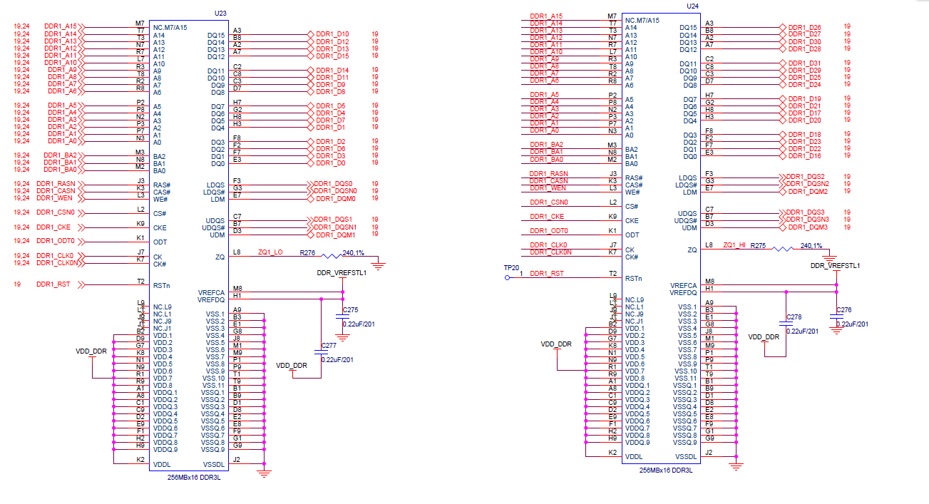
Thanks, Yicheng

  • Hi Yicheng,

    This is only partially correct. If you check carefully you will see that data bits are swapped within the byte boundary. To say this differently - you may swap bits within the byte lane to facilitate PCB routing. Exception is for the least senior bit, which must not be swapped (this is DDR3 hardware leveling requirement). Additionally each byte lane must have the corresponding DM/DQS/DQSn signals routed correspondingly. Bit swapping is absolutely prohibited across bytes. Also the Address, Clock and Control signals must never be swapped.
  • Hi Biser,

    Thank you so much for your answer. Can this be considered as default encryption? By encryption, I mean the CPU will know which signal is connected to which data signal for reading and writing. The data will not be any different.

    Best, Yicheng
  • No, this is done only to facilitate PCB routing.
  • Hi Biser,

    Thank you for your reply. So you are saying that within the byte the signals can be swapped except the lease senior bit, such as DQ0 and DQ8 for the lower byte and upper byte. Am I right? I am still wondering how the CPU can make sure the data will be correct if the signals are swapped, which basically lead the data stored in the memory is not the data the CPU intends to write. Let say the CPU wants to write byte 8'b00001111, but the data stored in the DDR3 is somehow 8'b10011001.

    Thanks, Yicheng

  • Yicheng,

    Look at this from the processor point of view. If the processor writes 00001111b to a memory cell, it doesn't matter what is actually written in the memory after bit swapping, the important thing is that the processor will read back exactly 00001111b from this location. If you draw this example on paper you will see what I mean.

    To say this otherwise, if processor outputs 1 on bit 4, which goes to bit 7 of the DDR, then readback from bit 7 of the DDR will output the same value of 1 to bit 4 of the processor (same address location, of course).
  •  

    Biser Gatchev-XID said:
    Yicheng,

    Look at this from the processor point of view. If the processor writes 00001111b to a memory cell, it doesn't matter what is actually written in the memory after bit swapping, the important thing is that the processor will read back exactly 00001111b from this location. If you draw this example on paper you will see what I mean.

    To say this otherwise, if processor outputs 1 on bit 4, which goes to bit 7 of the DDR, then readback from bit 7 of the DDR will output the same value of 1 to bit 4 of the processor (same address location, of course).


    Hi Biser,

    Thank you so much. Now I understand this. 

    Best, Yicheng