This thread has been locked.

If you have a related question, please click the "Ask a related question" button in the top right corner. The newly created question will be automatically linked to this question.

PCM9211: no DOUT signal from S/PDIF receiver

Part Number: PCM9211

Hi

I am working on a design that uses the PCM9211 for S/PDIF input and output.

I am providing a 24.576 MHz clock into the XI pin and a suitable S/PDIF signal into input pin RXIN3, and I reset the chip(s) with a low pulse on their nRST pin.

I have an IIC connection and can read/write the registers and the reset values are as described in your datasheet.

I have changed register 0x34 to 0xC3 to select my input pin (RXIN3), all other registers keep their power-on RESET value.

I am monitoring the output pins SCK0, BCK, LRCK and DOUT expecting to see a decoded I2S version of my input.

The clocks are outputing perfectly correctly, and change frequency if I change the sampling rate of my S/PDIF transmitter from 44.1kHz up to 192 kHz

_BUT_ there is no data coming out of the DOUT pin.

I have tried changing register 0x6B to 0x11 to avoid any possibility of Automatiic selection confusing me with switching to the ADC (which I am not using).

Further confusion comes from registers 0x38 and 0x39 which both read as 0x00 - suggesting the incoming S/PDIF is "out of range" but if this is so why are the clock output pins tracking my S/PDIF generator ?

I hope you can suggest something that I can check to find out why I have no output data.

Thanks for your time

Kind Regards

PhilipJ

  • Hello Phillip,

    S/PDIF will not output to DOUT, it will output to either MPO0 or MPO1 as they describe under section 8.3.8.7.3 in the datasheet and you see more about pin assignments in section 8.3.8.8 .

    Best Regards,

    Carson

    Low Power Audio Apps

  • Hi Carson,

    thanks for replying to my question.

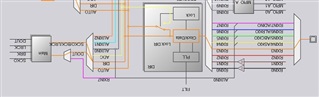
    I may not have explained myself too well, I am using the S/PDIF receiver (DIR) and expecting the decoded data stream to come out of the pin DOUT. This arrangement can be setup in the program "CodecControl" that is supplied by TI with the PCM9211 EVM board. Although I don't have the EVM board I have used the program to setup the routing I desire and see what it would set the internal registers to. I hope the image below comes through, sorry if it is upside down but I can't seem to get Windows 10 not to do this

    Anyway it shows what I'm trying to get sorted, but as I said originally, the clock outputs are working fine and change frequency if I change the sampling rate of my S/PDIF transmitting equipment but DOUT is just a flat low (it should be a -10dBFS 1kHz sine wave).

    The measured sampling rate in registers 0x38 (or 0x39) say that the incoming rate is "Out of range" but I have tried 48, 96 and 192 kHz with the same result. If the incoming signal is "out of range" would you expect the chip to still output the extracted clocks ?

    thanks for your time

    PhilipJ

  • Hello Philip,

    Are you making sure to adhere to the XTI pin clock requirement of supplying it before the PCM is powered up?

    Best,

    Carson

  • OK, that's a good point, no the clock comes in later because it is supplied by an FPGA which has to first be programmed. The chip is given a reset on it's nRST pin after the clock is applied, does this help ?

    What about the line that says "Once the XTI source clock is restored, the fs calculator resumes operation" - wouldn't this suggest that the clock can be presented after the chip has powered up ? If not what does this line actually mean ?

    Would this also prevent the data stream from appearing at the DOUT pin ?

    regards

    PhilipJ

  • Is it possible to have the clock supplied entirely before the device is powered on?

     "Once the XTI source clock is restored, the fs calculator resumes operation" this is just saying if clock stops and then you restore it then operation will resume but that is not directly related to having clock inputted before power which I believe is your issue and is what is stopping DOUT from outputting.

    -Carson

  • Unfortunatly this will not be possible with the current design so we will have to junk about $2500 dollars worth of prototype hardware.

    May I suggest that if this is such an important aspect to the operation of the device that it should be featured in large bold print near the beginning of the data-sheet and not just a small note on page 36.

    regards

    PhilipJ

  • Hey Philip,

    I am not 100% sure that is what stopping you from getting output, let me reach out to the engineers who used to be responsible for this part to see about a possible work around and/or what might actually be causing the problem. I am not expert on this part so I could be wrong.

    Best Regards,

    Carson

  • Hi Carson, thanks.

    I would appreciate any advice that can be obtained from the chip's design engineers that could help us rescue the expensive prototype hardware that we have built.

    I have myself been using the CodecControl program to see if there is any alternative routing that I could implement to get signals through the chip and onto our FPGA but so far nothing 100%

    I notice on the EVM board that the chip uses a crystal for the XTI signal, my past experience with crystal clocks is that they do take a finite amount of time to start-up and stabilise after power has been applied - dies this help in any way ?

    kind regards

    PhilipJ

  • Hi Philip,

    I am going to copy and paste the direct correspondence I got from my colleague.

    Hi Carson,


    The XTI clock source is not required for operation, It’s just used by the sampling frequency calculator and can be used as the clock source to the ADC. The only thing is if XTI is not stable and accurate, the PCM9211 may not calculate the correct sample rate, but again this will not actually impact it’s ability to decode the clocks or data. The calculator should resume operation once XTI is applied. The fact that they are not able to read this after supplying XTI suggests an issue with their input.


    You may also have them verify that their S/PDIF input is within the specified logic levels:


    Generally S/PDIF signals from coax connections are not within these levels because the protocol only requires a minimum of 0.2Vpp and maximum is 0.6Vpp, this is why the coax amplifiers are provided on RXIN0 and RXIN1. It’s possible the PLL is able to lock well enough and so the frequency is stable, but the logic levels are not met and so no data is decoded.


    Other things to double check would be the ground connection for the S/PDIF and possibly making sure that they have a 75 Ohm termination on their board. They may want to probe the S/PDIF signal at the board input to see if there are excessive reflections.


    Best,

    Zak

    Please review this and share with me if this helps resolve your problem

    Best Regards,

    Carson

  • Hi, thanks for the additional information. I have side-stepped the issues described with using coax S/PDIF as our design has an optical input device connected to RXIN3. I will however check the layout carefully to see that the integrity of the signal from this device is good.

    I have verified that the logic levels are acceptable by routing RXIN3 to RECOUT0 and then routing RECOUT0 to pin MPO0 where I have a TestPoint for the oscilloscope.

    I also checked the PLL by routing the LOCK signal to this same pin, l which initially was permanently high (I take this to mean un-locked ?). I used register 0x40 to power everything down/reset things (0x33), and then back to normal operation (0xc0), after which the LOCK signal (as seen on pin MPO0) was going up and down so maybe there is an issue with the circuit.

    I will investigate further

    Thanks to you and your colleague for the help

    PhilipJ

  • Hello Phillip

    No problem, let me know when you have more questions.

    Here is a little snippet from the datasheet talking about the PLL being locked or not

    Best Wishes,

    Carson