Hi Expert,
Customer is setting the external clocking from PPC3 with TLV320ADC3120 .
Normally, they will input 14.7456MHz clock to GPIO.
As irregular condition, they are considering about the condition of disabled clock generator to GPIO.
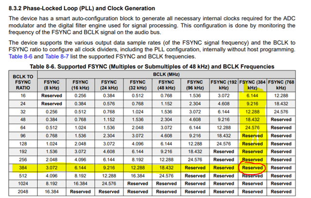
If the clocking input was enabled, they could confirm FSYNC=384kHz and normal operation same as customer settings.
However, if the clocking input was disabled, FSYNC was around 120kHz, also the device seems to send any data via I2S. The customer believed not work anything at no clocking.
Is it normal operation?
Also, could you please let me know the reason of output FSYNC at following conditions
- External clocking setting
- Not input clock (customer understand, it is irregular condition)
- Other input signals will be working and powered (other than clock signal)
Register setting is below,
| Page | Register Address | Register Name | Register Value |
| 0 | 0x00 | PAGE_CFG | 0x00 |
| 0 | 0x01 | SW_RESET | 0x00 |
| 0 | 0x02 | SLEEP_CFG | 0x81 |
| 0 | 0x05 | SHDN_CFG | 0x05 |
| 0 | 0x07 | ASI_CFG0 | 0x70 |
| 0 | 0x08 | ASI_CFG1 | 0x00 |
| 0 | 0x09 | ASI_CFG2 | 0x20 |
| 0 | 0x0A | ASI_MIX_CFG | 0x00 |
| 0 | 0x0B | ASI_CH1 | 0x00 |
| 0 | 0x0C | ASI_CH2 | 0x01 |
| 0 | 0x0D | ASI_CH3 | 0x02 |
| 0 | 0x0E | ASI_CH4 | 0x03 |
| 0 | 0x13 | MST_CFG0 | 0xc2 |
| 0 | 0x14 | MST_CFG1 | 0x79 |
| 0 | 0x15 | ASI_STS | 0xff |
| 0 | 0x16 | CLK_SRC | 0x10 |
| 0 | 0x1F | PDMCLK_CFG | 0xb0 |
| 0 | 0x20 | PDMIN_CFG | 0x00 |
| 0 | 0x21 | GPIO_CFG0 | 0xa2 |
| 0 | 0x22 | GPO_CFG0 | 0x00 |
| 0 | 0x29 | GPO_VAL | 0x00 |
| 0 | 0x2A | GPIO_MON | 0x00 |
| 0 | 0x2B | GPI_CFG0 | 0x00 |
| 0 | 0x2F | GPI_MON | 0x00 |
| 0 | 0x32 | INT_CFG | 0x00 |
| 0 | 0x33 | INT_MASK0 | 0xff |
| 0 | 0x36 | INT_LTCH0 | 0x00 |
| 0 | 0x3A | CM_TOL_CFG | 0x00 |
| 0 | 0x3B | BIAS_CFG | 0x00 |
| 0 | 0x3C | CH1_CFG0 | 0xa8 |
| 0 | 0x3D | CH1_CFG1 | 0x00 |
| 0 | 0x3E | CH1_CFG2 | 0x0b |
| 0 | 0x3F | CH1_CFG3 | 0x80 |
| 0 | 0x40 | CH1_CFG4 | 0x00 |
| 0 | 0x41 | CH2_CFG0 | 0xa8 |
| 0 | 0x42 | CH2_CFG1 | 0x00 |
| 0 | 0x43 | CH2_CFG2 | 0xc9 |
| 0 | 0x44 | CH2_CFG3 | 0x80 |
| 0 | 0x45 | CH2_CFG4 | 0x00 |
| 0 | 0x48 | CH3_CFG2 | 0xc9 |
| 0 | 0x49 | CH3_CFG3 | 0x80 |
| 0 | 0x4A | CH3_CFG4 | 0x00 |
| 0 | 0x4D | CH4_CFG2 | 0xc9 |
| 0 | 0x4E | CH4_CFG3 | 0x80 |
| 0 | 0x4F | CH4_CFG4 | 0x00 |
| 0 | 0x6B | DSP_CFG0 | 0x01 |
| 0 | 0x6C | DSP_CFG1 | 0x48 |
| 0 | 0x70 | AGC_CFG0 | 0x00 |
| 0 | 0x71 | GAIN_CFG | 0x00 |
| 0 | 0x73 | IN_CH_EN | 0x80 |
| 0 | 0x74 | ASI_OUT_CH_EN | 0xc0 |
| 0 | 0x75 | PWR_CFG | 0x00 |
| 0 | 0x76 | DEV_STS0 | 0x00 |
| 0 | 0x77 | DEV_STS1 | 0xc0 |
| 0 | 0x7E | I2C_CKSUM | 0xc2 |
| 1 | 0x00 | PAGE_CFG | 0x01 |
| 1 | 0x1E | VAD_CFG1 | 0x20 |
| 1 | 0x1F | VAD_CFG2 | 0x08 |
Thanks
Muk


