Dear Expert
This is schemetic. Attattached PCB layout.11-157011-02EN-V7POWER-V1.0.pdf

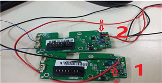
Two identical PCBS, both of which contain TPA2005D1DRBR circuit, were used. If the power amplifier chip on one board could work normally, the board was numbered as 1 and the power amplifier chip on the other board was coded as A; if the power amplifier chip on the other board could not work normally, the board was numbered as 2 and the power amplifier chip on the board was coded as B.Weld the 5V power cord, and fly the signal line at the same time to connect the chip 1 pin to the 5V for the test.
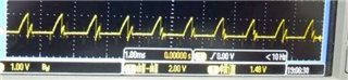
Use dc source for power supply of 5V, use signal source as signal input, and finally use oscilloscope to measure the waveform of the input end of two PCB power amplifier chips as follows:

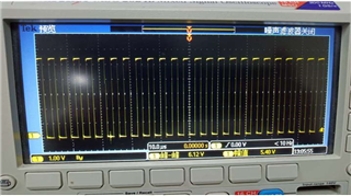
The output waveform of the two chips is as follows:
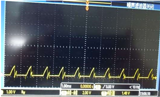
#1-A board waveform (the waveform of power amplifier chip A in normal operation) is as follows:
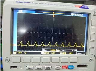
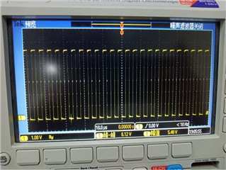
#2-B板子波形(功放芯片不能正常工作的波形)如下:
Switch the power amplifier chip (TPA2005D1DRBR) on the #1#2 board. Switch # 1-A and # 2-B before switching and # 1-B and # 2-A after switching.The measured power amplifier input waveform is unchanged, the output waveform is as follows.
#1-B waveform is as follows:
# 2-A waveform is as follows:
It can be seen that the switch between the power amplifier chip TPA2005D1DRBR can work normally, and the original abnormal board can work normally.
Expert ,could u give us more suggestion ,whether our schemtic or design have some problem?