This thread has been locked.

If you have a related question, please click the "Ask a related question" button in the top right corner. The newly created question will be automatically linked to this question.

PCMD3180: No register retention after software sleep

Part Number: PCMD3180

Hello, I experience that PCMD3180 registers are not retained when returning from software sleep mode.

The hardware sleep mode works fine (SHDNZ pin), configuration retention is not expected in that case obviously.

But I want to save on wakeup time, therefore I'd like to use software sleep mode and expect the settings to be retained.

I follow instructions of the datasheet (SBASA14 –MAY 2020) section 8.2.1.2 points 4 and 5.

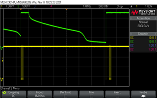
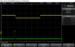
SHDNZ not touched at all, just the sleep register P0_R2 is written. It is confirmed by P0_R119 that sleep mode occurs. Current consumption also confirms this.

On wakeup, my application does not work.

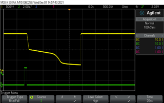
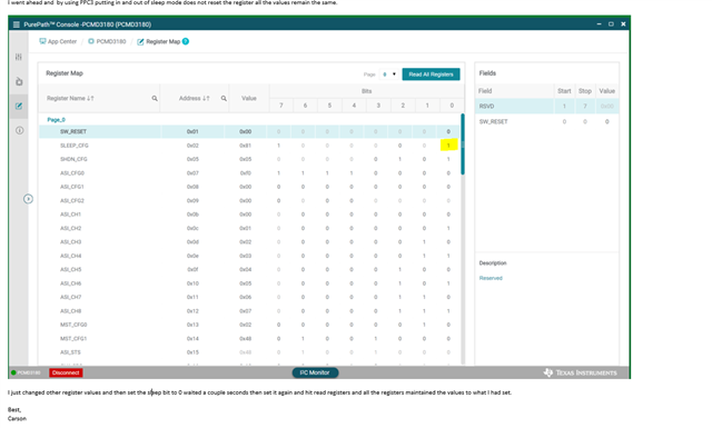
If reading back the registers, I see defaults. For instance, register 0x07 holds value 0x30, although was value 0x40 just before sleeping. I see default for other registers too.

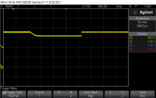
I have tried to keep my MCU completely up and running during the SW sleep mode, to be completely sure that no power loss occurs to PCMD3180.

But I experience the same, if SW sleep is longer than ~2s, registers fall back to defaults.

I expect retention based on section 7.4.2 (Sleep Mode or Software Shutdown)

"""In sleep mode or software shutdown mode, the device consumes very low quiescent current from the AVDD
supply and, at the same time, allows the I2C or SPI communication to wake the device for active operation.
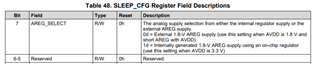
The device can also enter sleep mode when the host device sets the SLEEP_ENZ, P0_R2_D0 bit to 1'b0. If the
SLEEP_ENZ bit is asserted low when the device is in active mode, the device ramps down the volume on the
record data, powers down the analog and digital blocks, and enters sleep mode. However, the device still
continues to retain the last programmed value of the device configuration registers and programmable
coefficients."""

Do you have an idea what can be the case here? Shall I do any special configuration for the retention of registers?

  • Are you taking care for the Below?

    1.In sleep mode, do not perform any I 2C or SPI transactions, except for exiting sleep mode in order to enter active mode. After entering sleep mode, wait at least 10 ms before starting I 2C or SPI transactions to exit sleep mode.

    2.After entering active mode, wait at least 1 ms before starting any I 2C or SPI transactions in order to allow the device to complete the internal wake-up sequence.

  • Hello, thank you for the ideas. The suggested points 1 and 2 are considered.


    What I actually have now is:

    * I write SLEEP_CFG_SLEEP_ENZ_SLEEP to register SLEEP_CFG_ADDRESS.

    * Then wait 10ms.

    * Then stop I2S FSYNC and BCLK.

    At this time, the device is in software sleep mode.


    Then I wait 2 seconds, with a blocking call, so the main uC is powered normally. SHDNZ is not touched.


    Then I issue the wake command:

    * I write SLEEP_CFG_SLEEP_ENZ_ACTIVE | SLEEP_CFG_AREG_SELECT_INTERNAL into register SLEEP_CFG_ADDRESS.

    * Then I wait 5ms just to be sure

    * Enable FSYN and BCLK

    * Then wait 100ms to be extra sure

    * And start reading back the registers, which show all defaults.


    Do you have some idea what could cause loosing the configurations? Shall I maybe enable configuration retention somewhere, before enabling sleep?

  • I would suggest to try writing AREG_SELECT command also just before _CFG_SLEEP_ENZ _ACTIVE

    Also as an option try writing AREG_SELECT command 10ms before issuing  CFG_SLEEP_ENZ_ACTIVE

  • I have checked what you have suggested. Writing AREG_SELECT before the wakeup command does not help. The 10ms wait time does not make a difference either.

    I have checked very carefully, and have a few relevant observations:

    • After requesting the SW sleep mode, if I wait <1.5 sec before issuing the wakeup command, all the registers are retained OK. The low current consumption confirms that sleep mode is entered.
    • If sleep time is longer than ~1.5 sec, the registers are lost.
    • At ~1.5 sec, a very short current pulse is observed, its width is around 100usec, peaking at around 20 mA. This pulse then follows every 1.33 sec.
    • If sleep time is large enough to include this pulse, the registers are lost.
    • No voltage drop is visible on any of the lines (e.g. SHDNZ).
    • I have excluded other circuit parts causing the current pulse.
    • This current pulse seems to be the charge pulse to retain the registers. The pulse is not there if I use hardware sleep with SHDNZ.

    We use the typical application circuit as described in 8.2.1 of the manual. I have checked the caps values.


    Do you have any ideas for the case?

  • Is this pulse repeated as long Oankaj the commands are written r for  in sleep mode?  Does the pulse stop when you are woken up again?

  • Yes, the pulse repeats as long as being in sleep mode. When woken up, the pulses are not coming any longer. They are also not present in HW sleep mode (SHDNZ).

  • Have you checked the I2C Lines during the power down condition? Are you sure there is no I2C happening at this time.

    I also like to ask what voltage is given to AVDD Line? Is the current pulse you measure on AVDD line ? Take a look at the waveforms at AVDD and AReg line.

    If 3.3v is given to AVDD  then at the startup of the system power,  then AREG_SELECT should be set to 1. If for some reason the power is lost then system  can lose settings in sleep mode.

    you might try feeding AVDD and AREG with 1.8v. With this the I2Csetting for AREG_SELECT shall be 0 which is a default setting and any strange effect on  i2c should have no effect on power.

  • I have checked the I2C lines. There is no I2C activity after setting 0x80 to the SLEEP_CFG register. Next I2C activity is after the sleep period, wakeup command 0x81 to the SLEEP_CFG register. So I am sure about having no I2C activity during the sleep period. If sleep time is 1s, retention is OK. If sleep time is 2s or more, registers are lost.

    We follow the typical application circuit with 8 PDM mics, as shown in Fig161. Our VDD is 3.3V, also connected to AVDD. Measured to be 3.3365V, no glitch is visible. I have also tried supplying the VDD from a labs power supply. So AVDD is surely not lost during sleep.

    The current pulses were measured on the main VDD line, unfortunately connected to further places, like supplying the mics too. But if we use hardware sleep mode (SHDNZ), or back in active mode, the pulses are not present. Measuring current specifically on AVDD would be very difficult technically.

    The AREG line is measured to be 1.7857V in active mode, and starts falling slowly after the sleep command.  It falls below 1V at around 1.25s after the sleep command. On the wakeup command, AREG jumps back to 1.7857V immediately. See green curve on the attached scope recording.

    Interestingly, if I go with VDD=1.8V and AREG_SELECT=0 (external), and not connecting VDD to AREG, the retention is working OK. This is same if VDD = 3.3V is used.
    * If I use VDD=1.8V and AREG_SELECT=0 (external), and also connect 1.8V to the AREG pin, the registers are lost.
    * If I use AREG_SELECT=0 (external) and the AREG pin is not connected to 1.8V, the registers are retained. But if I change to AREG_SELECT=1 just on wakeup, the registers are lost.

    Our target is still using VDD=3.3V and the internal regulator.

    So you have any further ideas?

  • Is it correct that normally you use AVDD =3.3v and use the internal regulator to provide the 1.8v for AREG. ?This would mean that AREG_SELECT=1. 

    If i look at your waveform it seems that in sleep mode the 3.3v to 1.8v regulator is disconnected and just the 10u output capacitor on AREG pin is providing power. After about 1.25sec it falls below 1v. A larger capacitor would means a longer time then 1.25 sec.

    Are you setting AREG_SELECT TO 0 just before entering sleep?

    This action would disconnect the regulator 

    Can i also infer that you always lose data when you provide 1.8v externally?

  • We follow the typical application as shown in Fig161, so VDD=3.3V and AREG_SELECT=1. The sleep command is 0x80 and the wake command is 0x81, written to the SLEEP_CFG register. We are not setting AREG_SELECT to 0. The 1 MSB (0x80, 0x81) of the sleep and wake commands are the AREG_SELECT bit=1.

    The AREG pin voltage is indeed falling in SW sleep. The internal regulator keeps it at 1.8V before the sleep and after wakeup.
    Is the internal AREG regulator expected to hold the 1.8V on the AREG pin also in SW sleep mode?

    If we are using external 1.8V, and connect it also to the AREG pin, and using AREG_SELECT=0, the registers are lost.
    Interestingly, if we are not connecting the 1.8V to to the AREG, in this last configuration, the registers are retained.

  • Am I to understand that if you give AVDD=3.3V and keep AREG_SELECT=0 and do not connect 1.8v to AREG the data is retained for any amount of time when in sleep mode ?

    Can you please check the waveform on AREG pin to see what happens in this case in sleep?

    At the moment I am not sure what the AREG should be when in Sleep. To find this out we will have to locate the internal detail of the chip which may take time. We will look for this information if we have to.

  • Yes. If AREG_SELECT=0, and 1.8V is not externally connected to AREG, the registers are retained well. I have measured, and in this case AREG pin is at 0V continuously.

    Registers are lost if I connect the external 1.8V to AREG. or if I enable the internal regulator.

  • Does this fulfill your requirement?

  • Externally, we do not use AREG and MICBIAS. Just the capacitors are on, as in the reference design fig 161. The question here is, whether the PCMD3180 needs the AREG internally or not. If the PCMD3180 does not need the 1.8V on AREG, then we are probably fine.

    We use just PDM mics, as shown in the reference design.

  • I have checked: reading the microphones without the AREG results all-zeros, so does not work. So the PCM3180 needs the AREG, we cannot skip that.

  • You could consider to switch on internal regulators when the Mic is in use and switch off just befrore going to sleep. Lets say. the settings are loaded into the chip and we toggle the ARG_SELECT without invoking sleep. Do we lose settings?

  • I have tried initializing with internal areg, then switching to external areg 10ms before switching to sleep. On wakeup, I experience that the settings are lost.

    Considering using just the internal analog regulator, as the reference design describes, what should be the waveform on the AREG pin before-during-after the software sleep? Is it normal what I've seen on the scope screenshot?

  • Shall reply on monday

  • Lets say there is no external Regulator 1.8v input .Only 3.3v input supply is present

    We start with AREG_SELECT=1  and Load settings .

    10ms before sleep we make AREG=0.

    Go to Sleep

    wake up.

    Check if settings are OK

    Wake up  internal regulator with AREG_SELECT=1

    Check Mic

    ---------

    does the above work?

    If in sleep the AREG pin has no power source its voltage shall go to zero.

  • On power up, I wake the hardware with I2C Write addr=0x02 data=0x81, then configure all the registers. The microphones work.

    For sleep, I set AREG_SELECT=0 by I2C Write addr=0x02 data=0x01, then wait 10ms, and I2C Write addr=0x02 data=0x00.

    Wakeup is done with AREG_SELECT=1, so  I2C Write addr=0x02 data=0x81.

    The registers are lost, the mics don't work, regardless the length of the sleep.

    Same if wakeup is done with I2C Write addr=0x02 data=0x01, wait 10ms, then I2C Write addr=0x02 data=0x81.

    The AREG pin has no power source, and it goes to zero, as the scope screenshot has shown before.

    If I do not set AREG_SELECT=0 before sleep, the registers are retained OK if the length of the sleep period is less than about 1.5s.

  • Here is some speculation: I may be incorrect.

    I looked through our entire mail chain and I get a feeling that a substantial  Rising Edge on the AREG Pin or a low level seems to create a trigger that resets saved settings.

    Also, if we have a 3.3v supply  AREG_SEL=0 might be deemed an illogical setting . Lets say we forget about AREG_SEL=0 and just focus on 0x80 to Sleep and 0x81 to wake as you had tested before.. The datasheet says use AREG_SEL=1 with 3.3v

    In the case of sleep, it looks that the IC automatically disconnects AREG with the sleep command and expects us to reconnect AREG By giving AREG_SEL=1 at the moment of wakeup.. When this disconnection happens the voltage on the cap starts falling. In time period less then 1 sec there is a residual value on AREG  and when we turn on AREG at exit of sleep mode the level or the step is not enough to generate a reset of settings condition. If we wait more then 1 sec when we turn on the level or step is enough to create a transition.

    When we made AREG_SELECT=0 we never made a rising transition on AREG to reset saved settings.

    If the AREG pin during sleep dropped from 1.8v to say 1.2v then perhaps when we come out of sleep we dont have a level or transition that creates a reset of saved settings. Perhaps as a test we take a 1.8v supply and with a 1n4148 diode Positive connected to 1.8v and negative to  AREG PIN. When the device is in sleep this will clamp to AREG pin to 1.8v-0.6v or 1.2v . Perhaps this prevents a big transition on AREG pin on exit from sleep and savings might be retained.

    Please let me know your opinion.

  • I have made the suggested test with the diode. Now I use 0x80 and 0x81 to sleep and wake, so the internal regulator is in use, as expected.

    AREG starts to fall on sleep, as before, but clamped by the added external diode now. So it is forced not to fall below a level, see screenshot. The register settings are lost.

    Do you have any further idea what could cause the loss of the settings in software sleep mode?

  • Thank You fror trying this out. Can you also try below

    Turn on Internal regulator

    Write software Settings.

    Turn off Internal Regulator

    wait 2 sec

    Turn on Internal Regular

    Check if settings are retained.

    I am sorry for the extensive debugging requests. 

  • So, after configuring the registers and running on internal regulator, I just wrote 0x01 (active mode, external reg), wait 2 seconds, then 0x81 (active mode, internal reg).

    Without the diode clamping, AREG starts falling when changing regulator to external. After setting back to internal, the registers are not retained. (see scope recording)

    With the clamping diode, AREG falls just to the clamp level, then back when returning to internal regulator. In this case, the registers are retained OK. (see scope recording)


  • Thank You..

    if the 2sec was 1 minute does it still work with the diode?

    Some Questions:

    1. Are you using your own board or is the test done on a TI EVM?

    2. What is the value of the Supply Decoupling Capacitor on the Input Vcc line? Can you also send me your schematic?

       One other possibility is that when we actually try to switch on the regulator with the AREG Capacitor discharged completely there is an inrush of current from the 3.3v input line to charge this capacitor.. if there is inadequete decoupling capacitance between 3.3v and GND Pin there might be a dip on the 3.3v line and this may lead to a Power on Reset. I would also suggest to try the same test with a 22uf capacitor placed close between the Vcc and Gnd pin of the chip. 

    3.. Is it possible to send me a Dump of the Registers Before and after loss of data?

    I checked with the design teams here and they say that normally there should not be an issue with retention of data in sleep mode.. I am trying to locate a board so that we can try this ouit here.

  • I have tried the 'external regulator with clamping diode on AREG pin' case with 60 seconds wait. Retention works ok.

    We are using our own board. At the moment, I couldn't get an approval on sharing the schematic. But this part of the circuit is just the same as in your typical application in datasheet 8.2.1

    I have checked the capacitors:
      AVDD has 1uF and 100nF
      AREG has 10uF and 100nF
      IOVDD has 10uF and 100nF
      DREG has 10uF and 100nF
      MICBIAS has 1uF
      So, just as the datasheet 8.2.1

    I have checked for voltage dips VDD earlier, as one of the first steps. Couldn't find any voltage drip or strange spike that would motivate a reset.

    We have added now a 33uF on the top of the 1uF on AVDD. I have tried with 'internal regulator and sw sleep mode', so sleep with 0x80 and wake with 0x81. Retention does not work.

    The dump of the registers, if retention works ok (time between 0x80 and 0x81 is 1 sec):

    Digital SW Sleep retention test
    [D] I2C Write addr=0x02 data=0x80
    [I] Exit software sleep mode
    [D] I2C Write addr=0x02 data=0x81
    [I] Read: I2S output mode
    [D] I2C Read addr=0x07 data=0x40
    [I] Read: Config of input sources CH1..CH8 as PDM input
    [D] I2C Read addr=0x3c data=0x40
    [D] I2C Read addr=0x41 data=0x40
    [D] I2C Read addr=0x46 data=0x40
    [D] I2C Read addr=0x4b data=0x40
    [D] I2C Read addr=0x50 data=0x40
    [D] I2C Read addr=0x55 data=0x40
    [D] I2C Read addr=0x5a data=0x40
    [D] I2C Read addr=0x5f data=0x40
    [I] Read: Config of GPO1..4 as PDMCLK
    [D] I2C Read addr=0x22 data=0x41
    [D] I2C Read addr=0x23 data=0x41
    [D] I2C Read addr=0x24 data=0x41
    [D] I2C Read addr=0x25 data=0x41
    [I] Read: Config of GPI1..4 as PDMIN
    [D] I2C Read addr=0x2b data=0x45
    [D] I2C Read addr=0x2c data=0x67
    [I] Read: Enabled PDM input channels
    [D] I2C Read addr=0x73 data=0xff
    [I] Read: Config of CH5,6,7,8 to Right 1-2-3-4
    [D] I2C Read addr=0x0f data=0x20
    [D] I2C Read addr=0x10 data=0x21
    [D] I2C Read addr=0x11 data=0x22
    [D] I2C Read addr=0x12 data=0x23
    [I] Read: Enabled I2S channel slots
    [D] I2C Read addr=0x74 data=0xff
    [I] Read: Setting of PDMCLK divider
    [D] I2C Read addr=0x1f data=0x42
    [I] Read: Setting HPF filer
    [D] I2C Read addr=0x6b data=0x01
    [I] Read: Power up PDM Channels
    [D] I2C Read addr=0x75 data=0x60
    [I] Autodetect FSYNC
    [D] I2C Read addr=0x15 data=0x16

    The dump of the registers, if retention does not work (time between 0x80 and 0x81 is 2 sec):

    Digital SW Sleep retention test
    [D] I2C Write addr=0x02 data=0x80
    [I] Exit software sleep mode
    [D] I2C Write addr=0x02 data=0x81
    [I] Read: I2S output mode
    [D] I2C Read addr=0x07 data=0x30
    [I] Read: Config of input sources CH1..CH8 as PDM input
    [D] I2C Read addr=0x3c data=0x00
    [D] I2C Read addr=0x41 data=0x00
    [D] I2C Read addr=0x46 data=0x00
    [D] I2C Read addr=0x4b data=0x00
    [D] I2C Read addr=0x50 data=0x00
    [D] I2C Read addr=0x55 data=0x00
    [D] I2C Read addr=0x5a data=0x00
    [D] I2C Read addr=0x5f data=0x00
    [I] Read: Config of GPO1..4 as PDMCLK
    [D] I2C Read addr=0x22 data=0x00
    [D] I2C Read addr=0x23 data=0x00
    [D] I2C Read addr=0x24 data=0x00
    [D] I2C Read addr=0x25 data=0x00
    [I] Read: Config of GPI1..4 as PDMIN
    [D] I2C Read addr=0x2b data=0x00
    [D] I2C Read addr=0x2c data=0x00
    [I] Read: Enabled PDM input channels
    [D] I2C Read addr=0x73 data=0xf0
    [I] Read: Config of CH5,6,7,8 to Right 1-2-3-4
    [D] I2C Read addr=0x0f data=0x04
    [D] I2C Read addr=0x10 data=0x05
    [D] I2C Read addr=0x11 data=0x06
    [D] I2C Read addr=0x12 data=0x07
    [I] Read: Enabled I2S channel slots
    [D] I2C Read addr=0x74 data=0x00
    [I] Read: Setting of PDMCLK divider
    [D] I2C Read addr=0x1f data=0x40
    [I] Read: Setting HPF filer
    [D] I2C Read addr=0x6b data=0x01
    [I] Read: Power up PDM Channels
    [D] I2C Read addr=0x75 data=0x00
    [I] Autodetect FSYNC
    [D] I2C Read addr=0x15 data=0x16

  • IT IS SURPRISING THAT THE DIODE ALLOWS RETENTION OF SETTINGS WHEN OUT OF SLEEP BUT NOT IN SLEEP.

    Have you tried waiting for some time after exiting sleep to enable the regulator? Maybe 1 sec..

    Maybe you could exit sleep and check if settings are OK then wait 1 sec and then enable the Regulator then recheck

  • Indeed, registers survive the regulator switch in active mode, if the areg voltage is clamped by the diode. Looses settings in SW sleep mode.

    To be extra sure, I have repeated these cases:

    First, device is powered up with internal regulator+active mode, the configurations are set.

    Then, "sleep command"->wait>"wakeup command":

    Without diode: External regulator + sleep -->2sec--> Internal regulator + active : registers are lost
    With diode: External regulator + sleep -->2sec--> Internal regulator + active : registers are lost

    Without diode: External regulator + active -->2sec--> Internal regulator + active : registers are lost
    With diode: External regulator + active  -->2sec--> Internal regulator + active: registers retained OK


    As suggested, I have also added a 1 sec extra delay before enabling the internal regulator:

    Without diode: External regulator + sleep -->2sec--> External regulator + active -->1sec--> Internal regulator + active : registers are lost
    With diode: External regulator + sleep -->2sec--> External regulator + active  -->1sec--> Internal regulator + active : registers are lost

    In these latter cases, I have also checked the settings before the extra 1sec delay, but they are not there by then.

    I would focus on internal regulator cases, as we won't have external supply for the areg pin. How is the retention supplied in sleep mode?
    Does it make a difference internally, if we go to sleep with the internal or external regulator setting?

    I am really curious if retention works on your side with the evalkit.

  • What exactly do you mean by External Regulator in these tests?

  • in these tests, the sequence of issued commands were meant, as issued to SLEEP_CFG_ADDRESS.

    So "External regulator" is is the MSB of 0x00, while "Internal regulator" is 0x80.  Similarly, "Sleep" is LSB of 0x00, while "Active" is 0x01.

  • Would it be possible to take a look by just using 0x80 To Sleep and 0x81 To wake.

    Never turn off Internal regulator.

  • I am trying to Locate an EVM to do this test . Out Chip design people say that loss of settings should not occur.  

    Can you send to me the I2C commands you loaded so that i can try the same?

  • Ok, so using only the internal regulator, so commands 0x80 and 0x81. Never turning off the regulator. And the clamping diode is not supplied.  Behaviour is just before. Below you can find:

     * the sequence of write commands used for configuration

     * the sleep and wakeup commands

     * reading back the previously configured settings.

    I am really excited whether it works on the EVM.

    [I] Exit hardware sleep mode
    [I] Exit software sleep mode
    [D] I2C Write addr=0x02 data=0x81
    [I] Set I2S output mode
    [D] I2C Write addr=0x07 data=0x40
    [I] Configure input sources CH1..CH8 as PDM input
    [D] I2C Write addr=0x3c data=0x40
    [D] I2C Write addr=0x41 data=0x40
    [D] I2C Write addr=0x46 data=0x40
    [D] I2C Write addr=0x4b data=0x40
    [D] I2C Write addr=0x50 data=0x40
    [D] I2C Write addr=0x55 data=0x40
    [D] I2C Write addr=0x5a data=0x40
    [D] I2C Write addr=0x5f data=0x40
    [I] Configure GPO1..4 as PDMCLK
    [D] I2C Write addr=0x22 data=0x41
    [D] I2C Write addr=0x23 data=0x41
    [D] I2C Write addr=0x24 data=0x41
    [D] I2C Write addr=0x25 data=0x41
    [I] Configure GPI1..4 as PDMIN
    [D] I2C Write addr=0x2b data=0x45
    [D] I2C Write addr=0x2c data=0x67
    [I] Enable PDM input channels
    [D] I2C Write addr=0x73 data=0xff
    [I] Configure CH5,6,7,8 to Right 1-2-3-4
    [D] I2C Write addr=0x0f data=0x20
    [D] I2C Write addr=0x10 data=0x21
    [D] I2C Write addr=0x11 data=0x22
    [D] I2C Write addr=0x12 data=0x23
    [I] Enable I2S channel slots
    [D] I2C Write addr=0x74 data=0xff
    [I] Setting PDMCLK divider
    [D] I2C Write addr=0x1f data=0x42
    [I] Setting HPF filer
    [D] I2C Write addr=0x6b data=0x01
    [I] Power up PDM Channels
    [D] I2C Write addr=0x75 data=0x60
    [I] Autodetect FSYNC
    [D] I2C Read addr=0x15 data=0x16

    Digital SW Sleep retention test
    [D] I2C Write addr=0x02 data=0x80
    [I] Exit software sleep mode
    [D] I2C Write addr=0x02 data=0x81
    [I] Read: I2S output mode
    [D] I2C Read addr=0x07 data=0x30
    [I] Read: Config of input sources CH1..CH8 as PDM input
    [D] I2C Read addr=0x3c data=0x00
    [D] I2C Read addr=0x41 data=0x00
    [D] I2C Read addr=0x46 data=0x00
    [D] I2C Read addr=0x4b data=0x00
    [D] I2C Read addr=0x50 data=0x00
    [D] I2C Read addr=0x55 data=0x00
    [D] I2C Read addr=0x5a data=0x00
    [D] I2C Read addr=0x5f data=0x00
    [I] Read: Config of GPO1..4 as PDMCLK
    [D] I2C Read addr=0x22 data=0x00
    [D] I2C Read addr=0x23 data=0x00
    [D] I2C Read addr=0x24 data=0x00
    [D] I2C Read addr=0x25 data=0x00
    [I] Read: Config of GPI1..4 as PDMIN
    [D] I2C Read addr=0x2b data=0x00
    [D] I2C Read addr=0x2c data=0x00
    [I] Read: Enabled PDM input channels
    [D] I2C Read addr=0x73 data=0xf0
    [I] Read: Config of CH5,6,7,8 to Right 1-2-3-4
    [D] I2C Read addr=0x0f data=0x04
    [D] I2C Read addr=0x10 data=0x05
    [D] I2C Read addr=0x11 data=0x06
    [D] I2C Read addr=0x12 data=0x07
    [I] Read: Enabled I2S channel slots
    [D] I2C Read addr=0x74 data=0x00
    [I] Read: Setting of PDMCLK divider
    [D] I2C Read addr=0x1f data=0x40
    [I] Read: Setting HPF filer
    [D] I2C Read addr=0x6b data=0x01
    [I] Read: Power up PDM Channels
    [D] I2C Read addr=0x75 data=0x00
    [I] Autodetect FSYNC
    [D] I2C Read addr=0x15 data=0x16

  • Thanks, Shall respond in some time

  • Is there any update on the topic? Could you please check by next Monday?

  • We have requested one of our engineers to do this Test. he has promised to take this up as soon as he gets free from his current task.

    I shall try to ask him about his status

  • Thank you. Would be great to resolve this issue in the coming days.

  • I am including a snapshot of the e mail sent by our TI Engineer Carson. It seems he is able to

    retain values. AREG_SELECT=1 . It looks like internal regulator is in use. I have asked him to try to confirm

    if not external 1.8v is given on AREG pin. In addition he is to take the waveform on AREG pin when we move in and out of sleep.

    if we confirm that the system is operating on 3.3v Only then it may be a layout issue creating a reset when the regulator powers back on after wakeup from sleep

  • Thank you for the info. Please check and confirm that hardware configuration is the same as in your datasheet / 8.2.1 typical application. 

    If confirmed, and it works ok on your side, we will order the eval kit to check for the difference on our side.

  • Could you pls. also write me which exact evaluation kit do you use? I would order the same to compare the actual case.

  • have requested for the evm number. Should hopefully get info soon

  • I wish a Happy and healthy  new year to you and your family..

    Is there a TI Field representative with whom you are interacting. If so can you let me know his name so that we can try to set up the process that the board gets to you.

  • Same good wishes to you! Happy new year!

    We have no field representative. I have checked with the colleagues around, and it seems we have no TI field representative.

  • OK. In that case can you give me your address and shipping details . let me ask how 

    we can get this EVM to you.

  • My shipping address is the following:

    Roland Gémesi
    Silicon Labs
    Graphisoft Park, Ángel Sanz Briz út 13.
    SP2 Building
    1033 Budapest, Hungary

  • ok. shall get back in a bit

  • We need the below information:

    1. E-Mail

    2. Telephone 

    3. Some information on  Application where chip is used

  • E-Mail: roland.gemesi@silabs.com

    Telephone: +36304580604

    Application: Microphone array demonstrator