Because of the Thanksgiving holiday in the U.S., TI E2E™ design support forum responses may be delayed from November 25 through December 2. Thank you for your patience.

This thread has been locked.

If you have a related question, please click the "Ask a related question" button in the top right corner. The newly created question will be automatically linked to this question.

PCM4104: No Output

Part Number: PCM4104

I am developing with the PCM4104 on a custom board, but I am not getting any output.  I am expecting a 1 kHz sine wave.

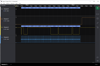
Here is my SPI configuration (after software reset):
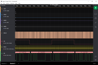
I am sending 24-bit I2S audio data (full scale 24-bit sinusoid):
This is the schematic of the part:
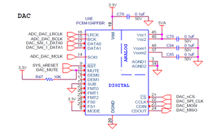
Voltage references are +5 / GND.

Any help at all would be greatly appreciated.

Bill

  • Hello, can you pull down the mute and see what happens? in first glance it looks like you have muted the device.

    if the problem is still there, please configure the device in hardware mode and test it again, We can go from there if still it is not working.

    Regards,

    Arash

  • Arash,

    Thank you for responding.  I've just confirmed that the mute pin is indeed pulled down.

    I cannot reconfigure the device in hardware mode without pulling up the pin.  Is there anything else we can try first?  Are there any bits on Register 0 that would give us interesting test output?

    Regards,

    Bill

  • BTW, are there any power supply sequencing requirements for this chip?  The 5V supply is usually off, and turned on only when audio output is required.

  • Bill, Something is not correct as schematic shows MUTE is pulled HIGH and you confirmed it is pulled LOW, I think either there are many other discrepancies b/w your schematic and actual connections OR this is not the correct schematics.

    No power sequencing b/w digital and analog is mentioned, however here is the sequence that happens on Power up:

    On power up, the internal reset signal is forced low, forcing the PCM4104 into a reset state. The power-on reset circuit monitors the VDD, VCC1, and VCC2 power supplies. When VDD exceeds +2.0V (margin of error is ±400mV) and VCC1 and VCC2 exceed +4.0V (margin of error is ±400mV), the internal reset signal is forced high. The PCM4104 then waits for the system clock input (SCKI) to become active. Once the system clock has been detected, the initialization sequence begins. The initialization sequence requires 1024 system clock periods for completion. When the initialization sequence is completed, the PCM4104 is ready to accept audio data at the audio serial port. Figure 5 shows the power-on reset sequence timing. If the PCM4104 is configured for Software mode control via the SPI port, all control registers will be reset to their default state during the initialization sequence. In both Standalone and Software modes, the analog outputs for all four channels are muted during the reset and initialization sequence. While in mute state, the analog output pins are driven to the bipolar zero voltage, or VCC/2. ........

    Some register s such as Register 6: System Control Register can disable the channel, With same token, your clk set up , R/LJ and ... might not be correct.

    Also all it takes to stop the DAC's output   is one pin with incorrect connection.  Can you please send the full schematic with all connections so I can review it.

    Also please capture and send  the critical waveforms, such as all CLKs, RESET, ....

    Thanks,

    Arash

  • Arash,

    The DAC_MUTE net is connected to a microprocessor GPIO which pushes it down.

    The RESET signal (net SYS_nRESET) is pulled high by a voltage supervisor at board power-up.

    The other signals should be visible in the logic analyzer traces I sent previously.

    Regards,

    Bill

  • Bill, for debugging the issue, usually we need the full schematic to see  what is connected to each pin such as PU and PD resistors to pins such as FMT, FS and ... If you think the schematic is correct then we go by that.

    I don't know what you are doing with VREF+ or VREF-, is it connected to correct voltages? Do you read any voltage on VCOM? 

    Next step is to make sure you are writing correctly  into registers, few readback will be helpful to verify this,  specially registers such as reg 5 , 6 and 7.

    May be you can probe few critical signals and see if the part is coming out of reset: start from supplies , Chip select,  reset , along with all clks.  You want to make sure the clks are (1) valid and within the spec and (2) are generated as expected  by probing them (for example  I can not read the freq of MCLK from your plot)

    Regards,

    Arash

  • Arash,

    Thanks again for helping me out.  My colleague and I worked this problem over for a week before I posted; it is unlikely to be anything obvious.

    The FS and FMT pins are floating.  The MCLK frequency is 36.864 MHz, which I have verified.  VCOM is 2.5 volts.

    The registers in hexadecimal are:
    1   FF
    2   FF
    3   FF
    4   00
    5   80
    6   01
    7   01

    I did leave out the output sections, because they're rather boring:

    The outputs then feed directly into the reconstruction filter as depicted in the datasheet.

    Regards,

    Bill

  • Bill, I will  take a look at the register values  you provided and will let you know by Friday.   I would suggest to use pull up/down  resistors for floating pins. Please verify the freq of all clks (Fs, BCLK). 

    Regards,

    Arash

  • Arash,

     I would suggest to use pull up/down  resistors for floating pins.

    Why, ESD?

    I was going by Figure 20. Typical Software Mode Configuration in the datasheet, which shows the pins unconnected.

    Please verify the freq of all clks (Fs, BCLK). 

    FS is 96 kHz.  BLCK is 48 times that (4.608 MHz).

  • No , not for ESD. For debugging only.  I would put all the pins in a known state first   or simply need to read all related registers for make sure set up is right . I will check those registers by tomorrow.

    Regards,

    Arash

  • 1   FF       1111 1111    No attenuation 0.5x (255-255)=0dB
    2   FF       1111 1111   
    3   FF       1111 1111    
    4   00       0000 0000    Mute
    5   80       1000 0000   MUT4=muted, MUT(3:1)= ON  ,   Zero date Mute: Disabled, Phase : Noninv,   DEM : default
    6   01       0001 0000    no reset, all 4 ch powerdown disabled, single rate
    7   01       0001 0000    24-bit left justified, LRCKP:  LRCK Polarity Inverted, BCKE BCK Sampling Edge :Rising Edge

    I checked all registers and it seems everything is ok and I don't see anything out of ordinary, The only change I could suggest is to try I2S data and play with polarity  and edge option , basically the  register 7 values, to make sure they match with your source (such as AP) set up. 

    Regards,

    Arash


  • Arash,

    After thrashing around for a bit, I finally see *some* output.  I switched the settings to the 24-bit left-justified, and suddenly there is something on the output.

    I don't understand why this setting would work, but the I²S setting does not, since the two formats are basically the same.  Would you be willing to look at the logic analyzer trace above and tell me what the problem is?

    Bill

  • Hi Bill,

    Arash is out of office until tomorrow, but I recommend you send a trace of your Left Justified results so that it's easier to compare and contrast your results from your trace above.

    Thanks,

    Jeff

  • Sure thing.  Here is Left-Justified mode at 96 kHz, which produces a perfect sine wave.

    If all I do is switch the DAC to I²S mode, the output becomes flat.  Granted, I²S should have a one clock delay, but even adding that the output is still flat.

    Inconceivable.

    Regards,
    Bill

  • Thanks Bill,

    Arash will look at this tomorrow and follow up with you. Please wait to reply until he does.

    Thank you,

    Jeff

  • Bill, Now that you verified the board is working with left justified and 96KHz, Seems the problem was with the handshake  between your source and IC (per the register values.

     You need to  make sure when  you select the I2S format at the source, the registers are also programmed as I2S in your script  . AP is what mostly we use for our testing, assuming you are using AP as well, you have to be careful with  the options you select. For example if I invert the Wfm, my chip stops working but when I invert and use Bit wide pulse still it works. Other things that I mentioned before are fall/rising edge for data clk as well as edge sync to fall/rise.


    Kind regards,

    Arash

  • Arash,

    I don't have the AP tool.  My I²S settings match the datasheet, but I can change them randomly and see if anything makes a difference.

    Regards,

    Bill

  •  I think some minor difference between your source and device is causing it and you have to find it by trail.

    Arash