This thread has been locked.

If you have a related question, please click the "Ask a related question" button in the top right corner. The newly created question will be automatically linked to this question.

PCM5102A: THD+N has differences between left and right channel

Part Number: PCM5102A

Hello,

We used PCM5102A and found that there is differences of  THD+N between two channels. And we tested as following:

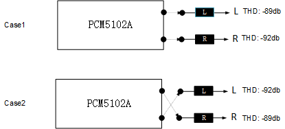
1. Change the back-ended of the DAC, and the THD+N is also changed, it indicated that the output  has inconsistency.

2. We have confirmed  the input I2S data are consistent.

Question:

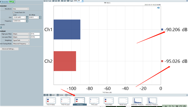
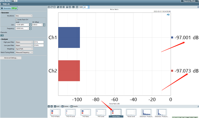
1. Why the two channels have different THD+N?(same noise floor).

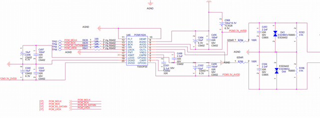
2. The schematic is as following. 

Best reagrds

Kailyn 

  • Hi Kailyn,

    Can you elaborate on what you mean by "Change the back-ended of the DAC, and the THD+N is also changed? " Do you mean you swap the connection for  outp and outn and the THD got better on the one that was worse,  and the one that was worse got better by doing so? if so, then it has to do with what is connected to  outputs.

    If not, How the analog waveforms compare for each channel  by visual inspection and by comparing fft on them for a given sinewave? 

    Is it possible to swap the inputs coming from you source for each channel and observe the outcome ( this is to  verify your inputs are identical and you get different distortion for different channels)

    Regards,

    Arash 

  • Hi  Arash,

    Thank you for your reply. I am sorry to make you confused about " Change the back-ended of the DAC, and the THD+N is also changed" .

    Please refer to the below diagram: 

    In addition, if swap the input, the output results are the same. And he has tried three PCM5102A and has the same results.

    So it looks like this kind of inconsistent is cause by the channel instead of input source or back ended.

    Please help to confirm.

    Best regards

    Kailyn 

  • Hi Kailyn,

    Today is a holiday for TI, so apologies for the delay. Arash will respond when he back in the office this coming Tuesday.

    Brian

  • Hi Brian,

    Thank you for your reply, and I am looking forward for your reply.

    Best regards

    kailyn 

  • Hello Kailyn,

    Thanks for confirming the that the degraded THD is always consistently present  on the LEFT channel. 

    I am still not convinced that it is created by the left channel for  all 3 DACs.

    To make sure, can you tell me how you are providing the input to the DAC? is the digital input provide to it via an ADC?

    If so, Can you send a 1KHz sinewave  to the DAC and do a FFT at the input of the DAC to make sure you are sending have  identical input to the DAC?

    An FFT at the output of the DAC will be useful too.

    Please also provide the schematic of the board so I can take a look at it.

    Regards,

    Arash

  • Hello Arash,

      The schematic has attached as above:

    And the customer  checked the two input are identical, and according to his description,  even  though he changed the input, the results are the same.

    Best regards

    kailyn 

  • Thanks Kailyn, I was asking  to see the schematic of the board  as the one they sent  originally was cut  at some point , specially I want to see what is connected to the output pin beyond what is showing here, just in case their loading is different.  Please also answer the above questions , I repeat them here:

    "To make sure, can you tell me how you are providing the input to the DAC? is the digital input provide to it via an ADC?

    If so, Can you send a 1KHz sinewave  to the DAC and do a FFT at the input of the DAC to make sure  you are sending   identical input to the DAC?

    An FFT at the output of the DAC will be useful too."

    If they are absolutely  satisfied the inputs are not  different ( by checking its fft ) , then it has to be the actual layout or output loading differences as I find it hard to believe 3 ICs have the same issue with one channel only.

    Regards,

    Arash

  • Hi Arash,

    Thank you for your reply.

    The customer sent me one video about  when he changed input and output SPDIF with AP.  The schematic is his tested board which is new design, please omit KT0642 section. The whole link is :

    AP555(SPDIF) -> Fiber->DEMO(WM8805)->PCM5102A-> LINEOUT->AP555(Unbalanced interface)

    The output load is AP, and he tried other different load, but the results are almost same.

    20220429-KT0642.pdf

    Best regards

    Kailyn 

  • Thanks Kailyn, I don't see anything out of ordinary in the schematic, so we might need to do few step by step debugging to figure it out.

    One thing that I would do is  to check the THD at L and R and compare it with THD at VOUTL and VOUTR.  I would also do not connect the connectors on J11 and repeat the above again ( in case the jumpers are connected) 

    And finally I would bypass the transceiver and directly go to the DAC via AP  and see if it makes any differences. If you go directly to DAC and monitor its output without any extra components ( except may be the filter/load) that can give us some idea if the mismatch is comping from outside of the DAC.

    Kind Regards,

    Arash