


Other Parts Discussed in Thread: TLV320ADC6140
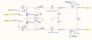

I' m from Tymphany EE and using the TLV320ADC5140 ADC for our amplifier.
Here I have a few question about the CMRR test condition definition and it's tolerance with different input level and frequency.
- The TLV320ADC5140 data sheet only state the CMRR typical is 60dB at 1KHz but doesn't mention the minimum and maximum. Does the testing condition are based on the DRE function disable?
- We want to know how the frequency ,input level and the threshold and maximum gain of DRE influence the CMRR result?
- what is CMRR work principle in ADC? We did measurement there is no DC offset between the balance input positive/ negative).How does it make the CMRR loose, Is it caused by the PGA gain tolerance?
- We found that the tlv320adc6140 has better noise performance 3dB better than tlv320adc5140 but both state the CMRR are same 60dB typical in spec. Can we also expect an improvement in the CMRR? Higher value or less variation?
- What reduction in CMRR is expected when DRE is enabled? At what signal levels?
Here is our debugging:
- We need the DRE function to improve the noise and our currently setting for DRE is -24dB Threshold and 20dB maximum gain. Based on the setting to measure the CMRR at 1KHz with100mVpp condition and found that the CMRR performance is a big variation from 46dB to 77dB between different CH and different chipset. After disable the DRE function then the CMRR variation smaller than before also can meet the spec typical 60dB(Check 5pcs sample).
- We try to reduce the DRE Threshold from -24dB to -54dB even down -66dB it doesn't to the CMRR.
- We try to reduce the DRE maximum from 20dB to 10dB it does to the CMRR but make the noise worse almost double can't meet our requirement. Then try to increase DRE maximum gain to 14dB to balance the CMRR and noise but the doesn't help to CMRR.
Thanks and waiting for your support!
