This thread has been locked.

If you have a related question, please click the "Ask a related question" button in the top right corner. The newly created question will be automatically linked to this question.

supported sample frequencies

Part Number: PCM1865

We are going to use PCM1865 in slave clocking mode, w/o SCK.

Our target sample frequency would be a multiple of 52.1kHz. This is outside the dedicated sample frequencies listed on table 11 (chapter 9.3.9.4.4 BCK Input Slave PLL Mode) and it's also outside the sample frequency ranges shown for register at address 0x73 (page 0) within the datasheet (32..48kHz,88,2..96kHz, 176,4..192kHz).

We tried to use a BCK ratio of 48 (LRCK=52,1kHz, BCK=2,5MHz) and a BCK ratio of 64 (LRCK=52,1kHz, BCK=3,334MHz). Both without success (sufficient sample values on the I2S output). Could the PCM1865 work using this setup?

Many thanks + best regards.

  • Hi,

    I have some clarifying questions. Does 0x75 return any kind of clocking errors? Do you mean that the data path is correct but is missing samples? How many samples are missing?

    Thank you,

    Jeff

  • Hi Jeff,

    thank you for the fast reply. As I read but now in the datasheet (sorry), there is an differentiation into two slave modes: "slave mode" and "slave PLL mode". Without considering this, I've used the "slave PLL mode", because I didn't supply a MCK (on SCKI pin). As result the PCM1865 has entered the "slave PLL mode", where non-standard audio rates are not supported (which we need: multiple of 52.1kHz - see above). Am I right?

    To answer your question: under the conditions described above I got 2 different scenarios:
    BCK ratio = 48
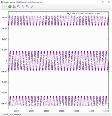
    → faulty samples (500Hz sine input, period within samples ok, but values not - see below), no errors within CLK_ERR_STAT:

    BCK ratio = 64
    → CLK_ERR_STAT register (0x75) returns errors on all 3 clocks alternately. Under these circumstances I didn't start sampling.

    Because of the finding above, this behavior not the point anymore (just only to answer your question).

    My current situation is, that master mode is not possible and we have to use as sample frequency a multiple of 52.1kHz. So, to use this non-standard audio sample frequency, I'll use the "slave mode" with a supplied MCK. Therefore I have some questions:

    1) Accord. to chapter 9.3.9.1 MCK has to be typically, a 2n power of the sampling rate (= SCK ratio). I would use SCK ratio = 256, which leads to SCK=13.34MHz, BCK=3.34MHz (BCK ratio = 64) and LRCK=52.1kHz (as my target sample frequency). All these clocks will be derived from one clock source, so they will be synchronous. And I will set CLKDET_EN to 0 (disable auto clock detection). Would you agree to this?

    2) Considering table 5 in chapter 9.3.9.4 PLL configuration is not necessary in the case above. But - in opposite to that for SW controlled device in (sub) chapters 9.3.9.4.2 and 9.3.9.4.5 is stated, that PLL has to be programmed manually (top of pages 38 and 45). I think there is a misunderstanding on my side... If I have to configure the PLL manually
    for the "Non-Audio MCK PLL Mode" as described in chapter 9.3.9.5, I would take MCK as PLLCKIN (=256*52.1kHz as described above). But what target value should I use for PLLCK (as clock frequency for the audio ADC and some other blocks)?

    Thank you again and best regards,
    Horst

  • Hi Horst,

    I agree with point 1. Though the PLL can still be used with non-audio standard clocks as long as the PLL is set correctly, like the note you pointed out mentions. The auto configuration is what is only supported by audio clock frequencies like the ones listed in Table 11. Chapter 9.3.9.5 is referring to situations where the MCLK is not a integer multiple (such as 256 or 128) of LRCLK. You can see on Table 10 and 13 that even a standard situation like 48kHz with a 256 ratio SCLK requires the PLL to satisfy the DSP and ADC core requirements on Table 8. 52.1k is close to 48k so I would use that as a guide. If you can generate a 512*fs MCLK then the PLL is off and everything can be done by simple dividers. For 256*fs you need the PLL to get the MCLK to a higher frequency such that you can satisfy Table 8.

    Best regards,

    Jeff

  • Hi Jeff,

    thanks. Table 8 was the essential hint. Although careful reading the data sheet, I ignored this. So the other tables became more understandable for me.

    Just for correction: my statement regarding "BCK ratio = 64" (2nd scenario) above was wrong, because of maloperation of the SPI master in that case. After fixing this, the PCM1865 now generates the expected output. Just the "BCK ratio = 48" (1st scenario) is still reproducable. But that may have other reasons, like misconfigured digital output (I2S/TDM format, ...)

    Summarizing your anwer above for me: we can't generate a MCK=512*fs. So I'll use the PLL to double MCK (as PLLCKIN w.r.t. chapter 9.3.9.5) and use MCK=256*fs. Keeping the default clock dividers for DSP1, DSP2 and ADC and switching their clock sources to "PLL", table 8 should be satisfied (DSP2 will get 512*52.1kHz).

    According table 5, LRCK/BCK direction is out, when the PLL is configured manually. I hope this will not conflict with my settings (MST_MODE=0 and above mentioned) or I mixed up cause and effect for that row.

    Best regards,
    Horst

  • Hi Horst,

    Since your MCLK is still a multiple of your LRCLK, I believe this still falls under Slave PLL mode in which case LRCLK and BCLK will still be outputs. Even then as long as your MST_MODE bit is correct LRCLK and BCLK should still be inputs.

    Best regards,

    Jeff

  • Hi Jeff,

    this confuses me. Why slave PLL mode, when I'm using an external MCK? (thought I had slave PLL mode before applying the MCK)
    And why should LRCK+BCK be outputs in slave (PLL) mode?

    I would use "slave mode": MST_MODE=0, MCK+LRCK+BCK as inputs, CLKDET_EN=0, clock ratios as described above. I thought I can double the MCK frequency (for DSP2) by the PLL, even when MCK is a multiple (256) of LRCK. From my understanding, MCK came into play because LRCK (52,1kHz) isn't a standard audio rate, which means going from slave PLL mode to slave mode accord. table 5.
    I am able to check it in a few days, so up to now that are assumptions only...

    My question was related to last row of table 5, which could mean that manual PLL configuration leads to BCK+LRCK as outputs (master mode only).

    Thank you + best regards,
    Horst

  • Apologies Horst,

    That was a typo. I meant to say LRCLK and BCLK will still be inputs.

    Best regards,

    Jeff

  • Hi Jeff,

    I tested my above mentioned settings, but the PCM1865 didn't come out from "clock waiting state" (bits 3..0 of reg 0x72 = 0001). Following are my clock config settings:

    reg. (page 0) value
    0x20 0x4E

    - SCK_XI_SEL: SCK
    - slave mode
    - clk source for DSP1/DSP2/ADC: PLL
    - CLKDET_EN: 0

    0x28 0x01 PLL ref: SCK
    PLL enabled
    0x29 0x00 PLL P divider: 1
    0x2A 0x01 PLL R multiplier: 2
    0x2B 0x01 PLL J integer part: 1
    0x2C 0x00 PLL D fract. part LSB: 0
    0x2D 0x00 PLL D fract. part MSB: 0
    0x21 0x00 DSP1 clock divider: 1  *
    0x22 0x01 DSP2 clock divider: 1/2  *
    0x23 0x03 ADC clock divider: 1/4  *

    *) default values don't match with data sheet

    The status regs (0x72..0x75, 0x78) report
    - state = clock waiting state
    - sampling frequency = 32..48kHz
    - the expected ratios: BCK=64, SCK=256
    - no clock errors for SCK, BCK and LCK (no Error and no Halt, reg 0x72 contains 0x00)
    - DVDD, AVDD and LDO: Good

    LRCK = 52.1kHz, BCK=3,334MHz, SCK=13.337MHz

    I didn't try any other PLL setting (P, R, J, D values) or another SCK_XI_SEL (other things I didn't see) up to now.
    But maybe you see the reason on the face of it Wink

    I noted that the PLL doesn't lock. According to the data sheet, corresponding bit (bit 4 of reg 0x28) is a R/W one (I think it should be read-only). But in both cases (writing 0 or 1 to bit 4) the behavior is the same (PLL doesn't lock).

    Hope, you can help.

    Best regards,
    Horst

  • Hi Horst,

    Today is a TI Holiday and our experts are out of office. Please give us another day to look at and answer your question. For record keeping purposes please do not reply to this message unless 48 hours have passed without a response.

    Thank you for your patience,

    Jeff

  • Hi Horst,

    Are you able to try the 48kHz use case from Table 13? I'd like to know if that works first and then try changing the clocks. The registers show there is some kind of clocking misconfiguration.

    Also make sure that in your current case, that the SCK_XI_SEL, like you mentioned, is set to SCK.

    Best regards,

    Jeff

  • (there was a typo in my reply above, I got no clock errors for SCK, BCK and LCK from reg 0x75)

    Hi Jeff,

    The non-locking state of the PLL was a result of subsequent re-programming of the above mentioned registers (including those for audio input selection, 0x06..0x09, not mentioned above). Only a power shutdown + reconfig led to a PLL locking state. After inserting a reset (0xFE @ 0x00) any reconfig leads to a locked PLL state. Tha't's now fixed, but the clock waiting state of the device is still there.

    Your suggestion, to try the 48kHz use case from Table 13 would be my next one. But just now I had a look at the conditions described in chapter 9.3.9.4.5:
    D = 0000,
    1 ≤ J ≤ 63 (matching my setup: J.D=1.0000(=K), P=1, R=2)
    1 MHz ≤ (PLLCKIN / P) ≤ 20 MHz, resp. 1 MHz ≤ 13.33MHz ≤ 20 MHz  Heavy check mark
    64 MHz < (PLLCKIN × K × R / P) < 100 MHz, resp. 64 MHz < 26.66MHz < 100 MHz   X

    So the 2nd condition is not satisfied. But I can't get out from the datasheet for which aim this conditions are given.
    I'll try
    to increase R to R=5, so both conditions should be satisfied. In that case DSP1 will run @ 66.7MHz and DSP2/ADC at the half/quarter of it.
    If that leads to come out of the clock waiting state, all should be fine and our target sample frequency (52.1kHz) should be used.

    Otherwise I'll try the 48kHz use case from Table 13 and stepwise change the clock (SCK).

    SCK_XI_SEL: I wrote 0x4E to reg. 0x20, so SCK should be selected as input for the mux "PLL_REF_SEL" (w.r.t. figures 33/44)
    PLL_REF_SEL: I wrote 0x11 to reg. 0x28, so the upper mux input (SCK_XI_SEL input) should be selected (here the lock flag is written - don't know if it's real writeable)

    In a few days I'm able to test the increased R multiplier for the PLL (and if necessary, the 48kHz use case from Table 13) and will tell you the result.

    Best regards,
    Horst

  • Hi Horst,

    Good catch on the PLL condition. That explains the clock error. Let me know what happens with the new settings.

    The lock flag probably can be overwritten and then changed once the state machine makes a change, but I'd keep it at 0 until the device flags it itself.

    Best regards,

    Jeff

  • Hi Jeff,

    today I tried following PLL setup to match the above mentioned 2nd condition (PLLCK=5* PLLCKIN=5* SCK):
    J.D=1.0000(=K), P=1, R=5
    This results in alternating states between Stand-By and Fade-IN of the device (checked in 1sec intervals).

    After that I tried (why "try"? see below...) this setup from the 48kHz example with BCK ratio 256 from Table 13 (PLLCK=8* PLLCKIN = 8* SCK):
    J.D=16.0000(=K), P=4, R=2
    This result now in running state of the device and first sample tests with our non-audio standard frequency (52.1kHz) seem to be ok. :)
    I hope the device stays stable, because using this setup
    is not satisfying the above mentioned 2nd condition (64MHz<8* 256*52.1kHz<100MHz).

    However - I don't understand why I have to "try". I thought, I can follow the datasheet (ch. 9.3.9.4.5 and the ratio conditions for BCC, SCK, DSP1/2, ADC) and the device should come into the running state. Maybe I overlooked another thing.

    Best regards,
    Horst

  • Hi Horst,

    I wouldn't keep the system violating the second condition. There might be some margin there but it would be best if we could get it satisfied. The alternating states are likely due to some clock error.

    Configuring a PLL by hand is pretty tricky and it's very easy to miss something. I put together an excel sheet to act like a calculator so that one can quickly determine if the PLL/DSP divider values are valid. I've attached it below. I did find that 5 won't provide a valid solution. But if you try 6, and adjust the dividers accordingly, you can get something that should work.

    PCM186xPLLCalculator.xlsx

    Best regards,

    Jeff

  • Hi Jeff,

    thanks again for your fast reply.
    I didn't had a look on the second condition as I took the 256* 48kHz setting from Table 13.

    Your suggestion, factor 6 for the PLL, works fine and led to a running device state with acceptable sample results for now.

    Also thank you for the excel sheet.
    This generates another question: how are the DSP/ADC divider values on cells G5/H5/J5 defined?
    In the text box you stated, that they may be changed that the resulting frequency satisfies the proper multiple of Fs. So this divider values need to be the half/same/double (for DSP1/DSP2/ADC) of the resulting (R*K)/P to fulfill this. On this point I may take "any" (R*K)/P result and find the matching dividers (G5/H5/J5). Assuming they need to be integers, the (R*K)/P result needs to be an even number and has to fulfill the PLL conditions (rows 15/16). Is this a plausibility check only? (would be missed in the datasheet...)

    On the other side this helps to find out that PLL factor 6 seems to be the only solution for our circumstances.

    Best regards
    Horst

  • Hi Horst,

    G5/H5/J5 are the divider values themselves. These are the values that you would write to the registers to program the divider values. The PLL clock is divided by that value and results in the clock frequency seen in Row 6. That value is then checked against the corresponding multiple of Fs by Table 8. Since the Table 8 dividers must be integers this results in the pattern you're seeing.

    Yes this just a plausibility check, to help determine what appropriate PLL/Divider values (if any) will provide a solution to the system based on the constraints given in the datasheet. It's consolidated and automatically calculated to make it easier than pen and paper. Some of our audio codecs have a PLL tool like this already made, so I made something similar to help with this situation.

    Glad to hear that the device is now running fine.

    Best regards,

    Jeff

  • Hi Jeff,

    thanks for your patience, my replies seem to be neverending... Wink

    I didn't write the G5/H5/J5 values to the registers to program the divider values for DSP1/DSP2/ADC. I wrote there the values 1/0.5/0.25, so these blocks should run with the corresponding divided PLLCK (80.025MHz/40.01MHz/20MHz) - maybe this was misunderstood by me. Table 8 says a multiple of output sampling rate and I used a multiple of PLLCK, not sure if output sampling rate is PLLCK or Fs. With respect to Table 13 the resulting frequencies are still within the allowed range for the DSPs and the ADC, fortunately.

    Thanks to your advice I will correct the divider value, so DSP1/2/ADC will run at the minimum required frequencies. If necessary, I have the possiblity to increase it by going back to the values before. I am able to check it in a few days.

    Best regards,
    Horst

  • Hi Horst,

    The paragraph just before 9.3.9.4 just says "sampling rate" (no mention of output) so I'm not sure why the table includes that language. Sometimes our codecs can operate the ADC and DACs at different sample rates but that's obviously not what's happening here. It may be referring to the sample rate of the digital data that is the output, which is redundant since there's only one sample rate that's relevant here. I'm certain it's referring to the frequency of the LRCLK.

    Table 8 is listed as a minimum requirement so since your dividers don't violate a minimum that may explain why it still works.

    Best regards,

    Jeff