This thread has been locked.

If you have a related question, please click the "Ask a related question" button in the top right corner. The newly created question will be automatically linked to this question.

TLV320ADC3101-Q1: Inquire about input high frequency frequency response control setting

Part Number: TLV320ADC3101-Q1
Other Parts Discussed in Thread: TLV320ADC3101,

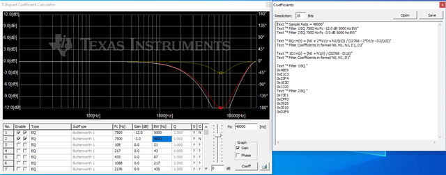
I would like to know what the equalizer settings are to reduce the frequency response in the 5Khz to 10 Khz band.

Please review and recommend the revised register settings of TLV320ADC3101 to resolve this issue asap.

Below are the currently applied setting values.

//###########################################################

           //# Clock configuration

          //# Master Mode

           //# MCLK as PLL input

           //# MCLK = 12MHz

           //# BCLK = 1.411MHz (44.1khz * 16bit * 2ch)

           //# WCLK = 44.1KHz = Fs

           //###########################################################

           //# Audio Settings          

           {0x34, 0x00 ,0x00},//# Select Page 0           

           {0x34, 0x01 ,0x01},//# Software reset required     

           {0x34 ,0x04 ,0x03},// # CODEC_CLKIN = PLL_CLK, PLL_CLKIN = MCLK

           {0x34 ,0x06 ,0x07},// # J=7

           {0x34 ,0x07 ,0x14},// # D=5264

           {0x34 ,0x08 ,0x90},// # D=5264


          // # P=1, R=1, PLL ON, PLL needs to be on before setting the NADC, MADC, AOSR and BCLK dividers

           {0x34 ,0x05 ,0x91},     


           {0x34 ,0x12 ,0x88},// # NADC = 8

           {0x34 ,0x13 ,0x82},// # MADC = 2

           {0x34 ,0x14 ,0x80},// # AOSR = 128

           {0x34 ,0x1B ,0x0C},// # I²S format, 16-bit data, Master mode*

           {0x34 ,0x1E ,0x88},// # BCLK Divider = ADC_CLK/8, ON


           //# Signal Processing Settings          

           {0x34 ,0x00 ,0x00},//# Select Page 0          

           {0x34 ,0x3d ,0x02},//# Set the ADC Mode to PRB_R2

           //#Biquad Setting    

            //{0x34 ,0x00 ,0x00},//# Select Page 0,  already in page 0         

            //{0x34 ,0x3d ,0x02},//# Select ADC Mode 2(PRB_R2) with 5 BQs/Chan, already written

            //{0x34 ,0x51 ,0x00},//# Power down Left ADC and Right ADC so that BQ Coefficients Can be   Downloaded, this is not required as this is the default state    


           //# Write BQ "A" = EQ, Fc=1000, 6, BW=200   

           {0x34 ,0x00 ,0x04},//# Select Page 4         

           //# Left An0         

           {0x34 ,0x0E ,0x77},

           {0x34 ,0x0F ,0x55},

           //# Left An1

           {0x34 ,0x10 ,0xb1},

           {0x34 ,0x11 ,0xc7},

           //# Left An2

           {0x34 ,0x12 ,0x65},

           {0x34 ,0x13 ,0xeb},

           //# Left Ad1

           {0x34 ,0x14 ,0x4e},

           {0x34 ,0x15 ,0x39},

           //# Left Ad2

           {0x34 ,0x16 ,0xa2},

           {0x34 ,0x17 ,0xbf},

           //{0x34 ,0x00 ,0x00 },//# Select Page 0         

           //{0x34 ,0x51 ,0x80},//# Left ADC powered up, Right ADC Powered down, power up ADC at the end after configuring PGA

           //{0x34 ,0x52 ,0x08},//#Mic Input Settings, power up ADC at the end after configuring PGA


           {0x34 ,0x00 ,0x01},//# Select Page 1         

           {0x34 ,0x33 ,0x60},//# MICBIAS1 = AVDD, MICBIAS2 Powered down      

           {0x34 ,0x3b ,0x32},//# Left Analog PGA Setting = +25dB

           //{0x34 ,0x3c ,0x80},//# Right PGA is muted, default setting

           {0x34 ,0x34 ,0xfc},//# Left ADC Input selection for Left PGA = IN1L(P) as Single Ended, 0dB

           //{0x34 ,0x37 ,0xff},//# Right ADC NOT connected mode, default setting


           {0x34 ,0x00 ,0x00},//# Select Page 0         

           {0x34 ,0x51 ,0x82},//# Left ADC powered up, Right ADC Powered down, soft-stepping disabled         

           {0x34 ,0x52 ,0x08},//# Left ADC ON, Right ADC OFF


};

  • Hi Hoonje,

    This looks identical to this thread: https://e2e.ti.com/support/audio-group/audio-internal/f/audio---internal-forum/1116317/tlv320adc3101-q1-frequency-response-issue-on-my-customer-s-system

    If this is your case, please refrain from creating multiple tickets. I apologize for any frustration. I will give a response to the original thread.

    Best regards,

    Jeff

  • Thank you for your answer.

    Please tell me how to use the TI Biquad Coefficient Calculator program.
    We want to attenuate the 5K to 10K frequency band by 15 dB.
    Please capture the example screen for setting the program and send it to me.

    Thank you.

  • Hi Hoonje,

    The Biquad tool allows you to draw your desired frequency response and then calculate the necessary coefficients.

    On each filter there is an enable column. The first switch determines if the filter contributes to the total result (in white) and the second switch will hide it from the plot, but still contribute to the total result. You can then select filter type (EQ, shelves, high and low pass, etc.). The next portions show the filter parameters like center frequency, bandwidth, and gain. These respond to clicking and dragging the filters on the frequency plot. Here I've entered in the parameters based on your desire to attenuate the 5k to 10k band by 15dB. Since each biquad can only achieve 12 dB, I have two filters imposed on each other to achieve the -15dB gain. This ADC has a limit of 5 biquads so you should design the filter within that limit. 

    On the bottom left of the screen there is the "Coeff" button. This will open the second window that displays the coefficients to be programmed in the register settings. There is the system parameters and the filters to be designed. The next two rows show the Biquad and 1st Order IIR transfer functions and in which order the coefficients will appear on the screen. The rows at the bottom are the coefficients themselves. Here you can see there are two filters (both biquads) and their coefficients are given in hex in the order N0,N1,N2,D1,D2. This window changes dynamically to any change on the original window.

    Best regards,

    Jeff

  • Thank you for your answer.

    We are using TLV320ADC3101-Q1 for our circuit.

    Which register of TLV320ADC3101-Q1 should I set the setting value that came out by pressing the "Coeff" button on the Biquad Coefficient Calculator?

  • Hi Hoonje,

    Table 9 on Page 37 of the datasheet outlines the relationship between the biquad coefficients and the register values they correspond to. The coefficient tool outputs the coefficients in the order N0, N1, N2, D1, D2 which is the same order as on Table 9. This is how you know which coefficient goes to which registers. You'll also notice your coefficients are 2 bytes wide. This is why the registers on Table 9 come in pairs. The first register is the MSB half and the second register is the LSB half.

    Best regards,

    Jeff

  • 1. There is no difference in the frequency response characteristics of the setting code you reviewed and the setting I made.

    2. When the biquad filter code you calculated was applied, the total dbV increased evenly. There was no decrease in the 5k-10K band.

    code volatile U8 Mic_Stting[39][3]=
    {
    //###########################################################
    //# Clock configuration
    //# Master Mode
    //# MCLK as PLL input
    //# MCLK = 12MHz
    //# BCLK = 1.411MHz (44.1khz * 16bit * 2ch)
    //# WCLK = 44.1KHz = Fs
    //###########################################################
    //# Audio Settings
    {0x34, 0x00 ,0x00},//# Select Page 0
    {0x34, 0x01 ,0x01},//# Software reset required
    {0x34 ,0x04 ,0x03},// # CODEC_CLKIN = PLL_CLK, PLL_CLKIN = MCLK
    {0x34 ,0x06 ,0x07},// # J=7
    {0x34 ,0x07 ,0x14},// # D=5264
    {0x34 ,0x08 ,0x90},// # D=5264

    // # P=1, R=1, PLL ON, PLL needs to be on before setting the NADC, MADC, AOSR and BCLK dividers
    {0x34 ,0x05 ,0x91},

    {0x34 ,0x12 ,0x88},// # NADC = 8
    {0x34 ,0x13 ,0x82},// # MADC = 2
    {0x34 ,0x14 ,0x80},// # AOSR = 128
    {0x34 ,0x1B ,0x0C},// # I²S format, 16-bit data, Master mode*
    {0x34 ,0x1E ,0x88},// # BCLK Divider = ADC_CLK/8, ON

    //# Signal Processing Settings
    {0x34 ,0x00 ,0x00},//# Select Page 0
    {0x34 ,0x3d ,0x02},//# Set the ADC Mode to PRB_R2
    //#Biquad Setting
    //{0x34 ,0x00 ,0x00},//# Select Page 0, already in page 0
    //{0x34 ,0x3d ,0x02},//# Select ADC Mode 2(PRB_R2) with 5 BQs/Chan, already written
    //{0x34 ,0x51 ,0x00},//# Power down Left ADC and Right ADC so that BQ Coefficients Can be Downloaded, this is not required as this is the default state

    //# Write BQ "A" = EQ, Fc=1000, 6, BW=200
    {0x34 ,0x00 ,0x04},//# Select Page 4
    //# Left An0
    {0x34 ,0x0E ,0x77},
    {0x34 ,0x0F ,0x55},
    //# Left An1
    {0x34 ,0x10 ,0xb1},
    {0x34 ,0x11 ,0xc7},
    //# Left An2
    {0x34 ,0x12 ,0x65},
    {0x34 ,0x13 ,0xeb},
    //# Left Ad1
    {0x34 ,0x14 ,0x4e},
    {0x34 ,0x15 ,0x39},
    //# Left Ad2
    {0x34 ,0x16 ,0xa2},
    {0x34 ,0x17 ,0xbf},
    //{0x34 ,0x00 ,0x00 },//# Select Page 0
    //{0x34 ,0x51 ,0x80},//# Left ADC powered up, Right ADC Powered down, power up ADC at the end after configuring PGA
    //{0x34 ,0x52 ,0x08},//#Mic Input Settings, power up ADC at the end after configuring PGA

    {0x34 ,0x00 ,0x01},//# Select Page 1
    {0x34 ,0x33 ,0x60},//# MICBIAS1 = AVDD, MICBIAS2 Powered down
    {0x34 ,0x3b ,0x32},//# Left Analog PGA Setting = +25dB
    //{0x34 ,0x3c ,0x80},//# Right PGA is muted, default setting
    {0x34 ,0x34 ,0xfc},//# Left ADC Input selection for Left PGA = IN1L(P) as Single Ended, 0dB
    //{0x34 ,0x37 ,0xff},//# Right ADC NOT connected mode, default setting

    {0x34 ,0x00 ,0x00},//# Select Page 0
    {0x34 ,0x51 ,0x82},//# Left ADC powered up, Right ADC Powered down, soft-stepping disabled
    {0x34 ,0x52 ,0x08},//# Left ADC ON, Right ADC OFF

    {0x34 ,0x00 ,0x04},//# Select Page 4
    {0x34 ,0x0E ,0x48},//# ADC Biquad Filter Coefficient, N0 Fillter, left Channel C7 Coefficient MSB Register 14
    {0x34 ,0x0F ,0xE9},//# ADC Biquad Filter Coefficient, N0 Fillter, left Channel C7 Coefficient LSB Register 15
    {0x34 ,0x10 ,0xE1},//# ADC Biquad Filter Coefficient, N1 Fillter, left Channel C8 Coefficient MSB Register 16
    {0x34 ,0x11 ,0xC3},//# ADC Biquad Filter Coefficient, N1 Fillter, left Channel C8 Coefficient LSB Register 17
    {0x34 ,0x12 ,0x23},//# ADC Biquad Filter Coefficient, N2 Fillter, left Channel C9 Coefficient MSB Register 18
    {0x34 ,0x13 ,0xF4},//# ADC Biquad Filter Coefficient, N2 Fillter, left Channel C9 Coefficient LSB Register 19
    {0x34 ,0x14 ,0x1E},//# ADC Biquad Filter Coefficient, D1 Fillter, left Channel C10 Coefficient MSB Register 20
    {0x34 ,0x15 ,0x3D},//# ADC Biquad Filter Coefficient, D1 Fillter, left Channel C10 Coefficient LSB Register 21
    {0x34 ,0x16 ,0x13},//# ADC Biquad Filter Coefficient, D2 Fillter, left Channel C11 Coefficient MSB Register 22
    {0x34 ,0x17 ,0x20},//# ADC Biquad Filter Coefficient, D2 Fillter, left Channel C11 Coefficient LSB Register 23
    {0x34 ,0x18 ,0x73},//# ADC Biquad Filter Coefficient, N0 Fillter, left Channel C12 Coefficient MSB Register 24
    {0x34 ,0x19 ,0xE1},//# ADC Biquad Filter Coefficient, N0 Fillter, left Channel C12 Coefficient LSB Register 25
    {0x34 ,0x1A ,0xCF},//# ADC Biquad Filter Coefficient, N1 Fillter, left Channel C13 Coefficient MSB Register 26
    {0x34 ,0x1B ,0xF0},//# ADC Biquad Filter Coefficient, N1 Fillter, left Channel C13 Coefficient LSB Register 27
    {0x34 ,0x1C ,0x39},//# ADC Biquad Filter Coefficient, N2 Fillter, left Channel C14 Coefficient MSB Register 28
    {0x34 ,0x1D ,0x25},//# ADC Biquad Filter Coefficient, N2 Fillter, left Channel C14 Coefficient LSB Register 29
    {0x34 ,0x1E ,0x30},//# ADC Biquad Filter Coefficient, D1 Fillter, left Channel C15 Coefficient MSB Register 30
    {0x34 ,0x1F ,0x10},//# ADC Biquad Filter Coefficient, D1 Fillter, left Channel C15 Coefficient LSB Register 31
    {0x34 ,0x20 ,0xD2},//# ADC Biquad Filter Coefficient, D2 Fillter, left Channel C16 Coefficient MSB Register 32
    {0x34 ,0x21 ,0xF9},//# ADC Biquad Filter Coefficient, D2 Fillter, left Channel C16 Coefficient LSB Register 33

    };

  • Hi Hoonje,

    ADCs must be powered down before biquads can be written and then the ADCs must be powered up again. You make note of this in your script but I'm not sure why you are writing to Page 4 twice at different times. I ran this attached script to configure the biquads after setting up the signal path and I was able to see the matching frequency response:


    w 30 00 00 //Page 0
    w 30 3D 02 //Set ADC Processing to PRB_R2
    w 30 51 00 //Power-down ADCs and digital mic inputs
    w 30 00 04 //Page 4
    //Calculated Biquad coefficients entered sequentially
    w 30 0E 5A C8 E0 26 29 8C 1F DA FB AC 6B 98 DE E0 50 99 21 20 C3 CF 7F FF 00 00 00 00 00 00 00 00
    w 30 2C 7F FF 00 00 00 00 00 00 00 00 7F FF 00 00 00 00 00 00 00 00
    w 30 4E 5A C8 E0 26 29 8C 1F DA FB AC 6B 98 DE E0 50 99 21 20 C3 CF 7F FF 00 00 00 00 00 00 00 00
    w 30 6C 7F FF 00 00 00 00 00 00 00 00 7F FF 00 00 00 00 00 00 00 00
    w 30 00 00 //Page 0
    w 30 51 C0 //Power on ADCs
    w 30 52 00 //Unmute ADCs

    Let me know if this works.

    Best regards,

    Jeff

  • As Jeff pointed out, after powering down the ADC, I wrote a biquad and powered the ADC back on.
    Please review the code.

    code volatile U8 Mic_Stting[39][3]=
    {
    //###########################################################
    //# Clock configuration
    //# Master Mode
    //# MCLK as PLL input
    //# MCLK = 12MHz
    //# BCLK = 1.411MHz (44.1khz * 16bit * 2ch)
    //# WCLK = 44.1KHz = Fs
    //###########################################################
    //# Audio Settings
    {0x34, 0x00 ,0x00},//# Select Page 0
    {0x34, 0x01 ,0x01},//# Software reset required
    {0x34 ,0x04 ,0x03},// # CODEC_CLKIN = PLL_CLK, PLL_CLKIN = MCLK
    {0x34 ,0x06 ,0x07},// # J=7
    {0x34 ,0x07 ,0x14},// # D=5264
    {0x34 ,0x08 ,0x90},// # D=5264

    // # P=1, R=1, PLL ON, PLL needs to be on before setting the NADC, MADC, AOSR and BCLK dividers
    {0x34 ,0x05 ,0x91},

    {0x34 ,0x12 ,0x88},// # NADC = 8
    {0x34 ,0x13 ,0x82},// # MADC = 2
    {0x34 ,0x14 ,0x80},// # AOSR = 128
    {0x34 ,0x1B ,0x0C},// # I²S format, 16-bit data, Master mode*
    {0x34 ,0x1E ,0x88},// # BCLK Divider = ADC_CLK/8, ON

    //# Signal Processing Settings
    {0x34 ,0x00 ,0x00},//# Select Page 0
    {0x34 ,0x3d ,0x02},//# Set the ADC Mode to PRB_R2
    {0x34 ,0x51 ,0x00},//# Power-down ADCs and digital mic inputs

    {0x34 ,0x00 ,0x04},//# Select Page 4
    {0x34 ,0x0E ,0x48},//# ADC Biquad Filter Coefficient, N0 Fillter, left Channel C7 Coefficient MSB Register 14
    {0x34 ,0x0F ,0xE9},//# ADC Biquad Filter Coefficient, N0 Fillter, left Channel C7 Coefficient LSB Register 15
    {0x34 ,0x10 ,0xE1},//# ADC Biquad Filter Coefficient, N1 Fillter, left Channel C8 Coefficient MSB Register 16
    {0x34 ,0x11 ,0xC3},//# ADC Biquad Filter Coefficient, N1 Fillter, left Channel C8 Coefficient LSB Register 17
    {0x34 ,0x12 ,0x23},//# ADC Biquad Filter Coefficient, N2 Fillter, left Channel C9 Coefficient MSB Register 18
    {0x34 ,0x13 ,0xF4},//# ADC Biquad Filter Coefficient, N2 Fillter, left Channel C9 Coefficient LSB Register 19
    {0x34 ,0x14 ,0x1E},//# ADC Biquad Filter Coefficient, D1 Fillter, left Channel C10 Coefficient MSB Register 20
    {0x34 ,0x15 ,0x3D},//# ADC Biquad Filter Coefficient, D1 Fillter, left Channel C10 Coefficient LSB Register 21
    {0x34 ,0x16 ,0x13},//# ADC Biquad Filter Coefficient, D2 Fillter, left Channel C11 Coefficient MSB Register 22
    {0x34 ,0x17 ,0x20},//# ADC Biquad Filter Coefficient, D2 Fillter, left Channel C11 Coefficient LSB Register 23
    {0x34 ,0x18 ,0x73},//# ADC Biquad Filter Coefficient, N0 Fillter, left Channel C12 Coefficient MSB Register 24
    {0x34 ,0x19 ,0xE1},//# ADC Biquad Filter Coefficient, N0 Fillter, left Channel C12 Coefficient LSB Register 25
    {0x34 ,0x1A ,0xCF},//# ADC Biquad Filter Coefficient, N1 Fillter, left Channel C13 Coefficient MSB Register 26
    {0x34 ,0x1B ,0xF0},//# ADC Biquad Filter Coefficient, N1 Fillter, left Channel C13 Coefficient LSB Register 27
    {0x34 ,0x1C ,0x39},//# ADC Biquad Filter Coefficient, N2 Fillter, left Channel C14 Coefficient MSB Register 28
    {0x34 ,0x1D ,0x25},//# ADC Biquad Filter Coefficient, N2 Fillter, left Channel C14 Coefficient LSB Register 29
    {0x34 ,0x1E ,0x30},//# ADC Biquad Filter Coefficient, D1 Fillter, left Channel C15 Coefficient MSB Register 30
    {0x34 ,0x1F ,0x10},//# ADC Biquad Filter Coefficient, D1 Fillter, left Channel C15 Coefficient LSB Register 31
    {0x34 ,0x20 ,0xD2},//# ADC Biquad Filter Coefficient, D2 Fillter, left Channel C16 Coefficient MSB Register 32
    {0x34 ,0x21 ,0xF9},//# ADC Biquad Filter Coefficient, D2 Fillter, left Channel C16 Coefficient LSB Register 33

    {0x34 ,0x00 ,0x00},//# Page 0
    {0x34 ,0x51 ,0xC0},//# Power on ADCs
    {0x34 ,0x52 ,0x00},//# Unmute ADCs

    //# Write BQ "A" = EQ, Fc=1000, 6, BW=200
    {0x34 ,0x00 ,0x04},//# Select Page 4
    //# Left An0
    {0x34 ,0x0E ,0x77},
    {0x34 ,0x0F ,0x55},
    //# Left An1
    {0x34 ,0x10 ,0xb1},
    {0x34 ,0x11 ,0xc7},
    //# Left An2
    {0x34 ,0x12 ,0x65},
    {0x34 ,0x13 ,0xeb},
    //# Left Ad1
    {0x34 ,0x14 ,0x4e},
    {0x34 ,0x15 ,0x39},
    //# Left Ad2
    {0x34 ,0x16 ,0xa2},
    {0x34 ,0x17 ,0xbf},
    //{0x34 ,0x00 ,0x00 },//# Select Page 0
    //{0x34 ,0x51 ,0x80},//# Left ADC powered up, Right ADC Powered down, power up ADC at the end after configuring PGA
    //{0x34 ,0x52 ,0x08},//#Mic Input Settings, power up ADC at the end after configuring PGA

    {0x34 ,0x00 ,0x01},//# Select Page 1
    {0x34 ,0x33 ,0x60},//# MICBIAS1 = AVDD, MICBIAS2 Powered down
    {0x34 ,0x3b ,0x32},//# Left Analog PGA Setting = +25dB
    //{0x34 ,0x3c ,0x80},//# Right PGA is muted, default setting
    {0x34 ,0x34 ,0xfc},//# Left ADC Input selection for Left PGA = IN1L(P) as Single Ended, 0dB
    //{0x34 ,0x37 ,0xff},//# Right ADC NOT connected mode, default setting

    {0x34 ,0x00 ,0x00},//# Select Page 0
    {0x34 ,0x51 ,0x82},//# Left ADC powered up, Right ADC Powered down, soft-stepping disabled
    {0x34 ,0x52 ,0x08},//# Left ADC ON, Right ADC OFF


    };

    Thank you

  • Hi Hoonje,

    I've made some edits to the code. Mostly getting rid of redundancies and placing the segments in the correct order.

    code volatile U8 Mic_Stting[39][3]=
    {
    //###########################################################
    //# Clock configuration
    //# Master Mode
    //# MCLK as PLL input
    //# MCLK = 12MHz
    //# BCLK = 1.411MHz (44.1khz * 16bit * 2ch)
    //# WCLK = 44.1KHz = Fs
    //###########################################################
    //# Audio Settings
    {0x34, 0x00 ,0x00},//# Select Page 0
    {0x34, 0x01 ,0x01},//# Software reset required
    {0x34 ,0x04 ,0x03},// # CODEC_CLKIN = PLL_CLK, PLL_CLKIN = MCLK
    {0x34 ,0x06 ,0x07},// # J=7
    {0x34 ,0x07 ,0x14},// # D=5264
    {0x34 ,0x08 ,0x90},// # D=5264

    // # P=1, R=1, PLL ON, PLL needs to be on before setting the NADC, MADC, AOSR and BCLK dividers
    {0x34 ,0x05 ,0x91},

    {0x34 ,0x12 ,0x88},// # NADC = 8
    {0x34 ,0x13 ,0x82},// # MADC = 2
    {0x34 ,0x14 ,0x80},// # AOSR = 128
    {0x34 ,0x1B ,0x0C},// # I²S format, 16-bit data, Master mode*
    {0x34 ,0x1E ,0x88},// # BCLK Divider = ADC_CLK/8, ON

    {0x34 ,0x00 ,0x01},//# Select Page 1
    {0x34 ,0x33 ,0x60},//# MICBIAS1 = AVDD, MICBIAS2 Powered down
    {0x34 ,0x3b ,0x32},//# Left Analog PGA Setting = +25dB
    //{0x34 ,0x3c ,0x80},//# Right PGA is muted, default setting
    {0x34 ,0x34 ,0xfc},//# Left ADC Input selection for Left PGA = IN1L(P) as Single Ended, 0dB
    //{0x34 ,0x37 ,0xff},//# Right ADC NOT connected mode, default setting

    //# Signal Processing Settings
    {0x34 ,0x00 ,0x00},//# Select Page 0
    {0x34 ,0x3d ,0x02},//# Set the ADC Mode to PRB_R2
    {0x34 ,0x51 ,0x00},//# Power-down ADCs and digital mic inputs

    {0x34 ,0x00 ,0x04},//# Select Page 4
    {0x34 ,0x0E ,0x48},//# ADC Biquad Filter Coefficient, N0 Fillter, left Channel C7 Coefficient MSB Register 14
    {0x34 ,0x0F ,0xE9},//# ADC Biquad Filter Coefficient, N0 Fillter, left Channel C7 Coefficient LSB Register 15
    {0x34 ,0x10 ,0xE1},//# ADC Biquad Filter Coefficient, N1 Fillter, left Channel C8 Coefficient MSB Register 16
    {0x34 ,0x11 ,0xC3},//# ADC Biquad Filter Coefficient, N1 Fillter, left Channel C8 Coefficient LSB Register 17
    {0x34 ,0x12 ,0x23},//# ADC Biquad Filter Coefficient, N2 Fillter, left Channel C9 Coefficient MSB Register 18
    {0x34 ,0x13 ,0xF4},//# ADC Biquad Filter Coefficient, N2 Fillter, left Channel C9 Coefficient LSB Register 19
    {0x34 ,0x14 ,0x1E},//# ADC Biquad Filter Coefficient, D1 Fillter, left Channel C10 Coefficient MSB Register 20
    {0x34 ,0x15 ,0x3D},//# ADC Biquad Filter Coefficient, D1 Fillter, left Channel C10 Coefficient LSB Register 21
    {0x34 ,0x16 ,0x13},//# ADC Biquad Filter Coefficient, D2 Fillter, left Channel C11 Coefficient MSB Register 22
    {0x34 ,0x17 ,0x20},//# ADC Biquad Filter Coefficient, D2 Fillter, left Channel C11 Coefficient LSB Register 23
    {0x34 ,0x18 ,0x73},//# ADC Biquad Filter Coefficient, N0 Fillter, left Channel C12 Coefficient MSB Register 24
    {0x34 ,0x19 ,0xE1},//# ADC Biquad Filter Coefficient, N0 Fillter, left Channel C12 Coefficient LSB Register 25
    {0x34 ,0x1A ,0xCF},//# ADC Biquad Filter Coefficient, N1 Fillter, left Channel C13 Coefficient MSB Register 26
    {0x34 ,0x1B ,0xF0},//# ADC Biquad Filter Coefficient, N1 Fillter, left Channel C13 Coefficient LSB Register 27
    {0x34 ,0x1C ,0x39},//# ADC Biquad Filter Coefficient, N2 Fillter, left Channel C14 Coefficient MSB Register 28
    {0x34 ,0x1D ,0x25},//# ADC Biquad Filter Coefficient, N2 Fillter, left Channel C14 Coefficient LSB Register 29
    {0x34 ,0x1E ,0x30},//# ADC Biquad Filter Coefficient, D1 Fillter, left Channel C15 Coefficient MSB Register 30
    {0x34 ,0x1F ,0x10},//# ADC Biquad Filter Coefficient, D1 Fillter, left Channel C15 Coefficient LSB Register 31
    {0x34 ,0x20 ,0xD2},//# ADC Biquad Filter Coefficient, D2 Fillter, left Channel C16 Coefficient MSB Register 32
    {0x34 ,0x21 ,0xF9},//# ADC Biquad Filter Coefficient, D2 Fillter, left Channel C16 Coefficient LSB Register 33

    {0x34 ,0x00 ,0x00},//# Select Page 0
    {0x34 ,0x51 ,0x82},//# Left ADC powered up, Right ADC Powered down, soft-stepping disabled
    {0x34 ,0x52 ,0x08},//# Left ADC ON, Right ADC OFF

    };

    Best regards,

    Jeff