This thread has been locked.

If you have a related question, please click the "Ask a related question" button in the top right corner. The newly created question will be automatically linked to this question.

OPA1622: enable feature not behaving as expected

Part Number: OPA1622

Hello All!

I'm experiencing a very odd behavior when trying to use the enable pin feature of the OPA1622 in the clipper circuit below:

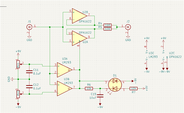
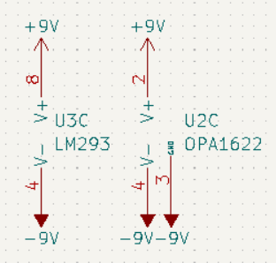
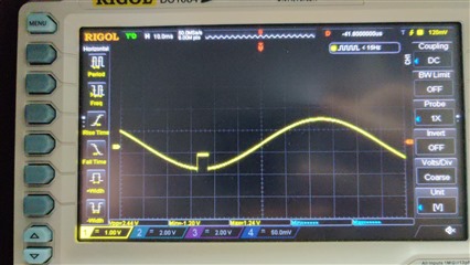
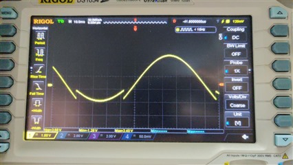
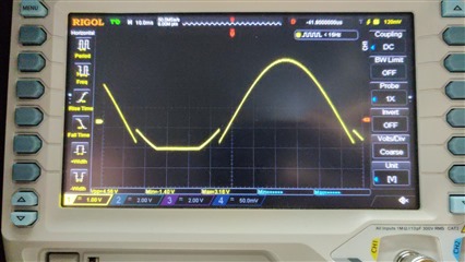
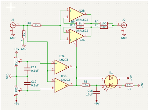
As can be seen above, I'm setting the GND pin to -9V in order to reference the enable signal to it.

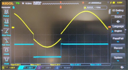
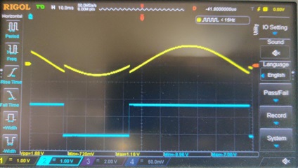
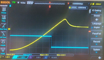
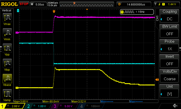
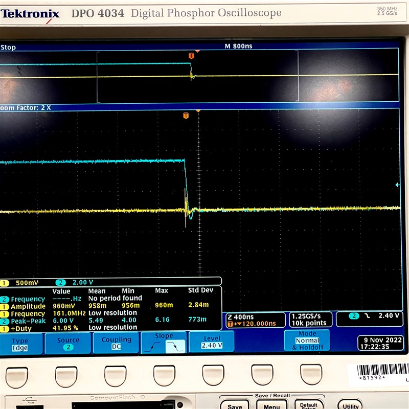
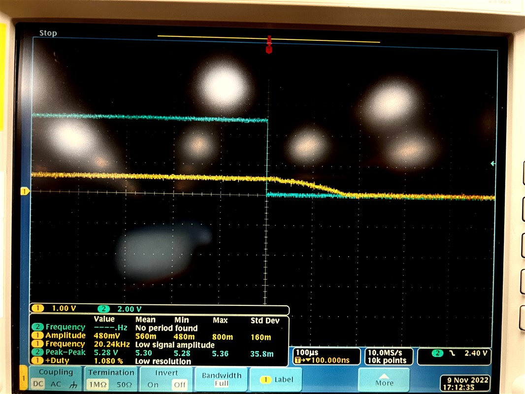
The enable signal generation (in cyan below) mechanism works as expected, but the OPA1622 output (in yellow below) does not:

I should also mention that I'm using 2 diode in series to protect the power supplies from inverting.

I'm a bit at a loss :) .

  • Hi Mathieu,

    I am pretty sure there is an error in the OPA1622 circuit connection in your circuit. The OPA1622 has a GND pin (pin 3) that must be connected to GND. The schematic provided shows it connected to -9 V. See datasheet Section 5 - Pin Configuration and Functions, and Figure 60 - Operational Amplifier Board Layout for a Difference Amplifier Configuration for more information about grounding pin 3.

    Regards, Thomas

    Precision Amplifiers Applications Engineering

  • Hello Thomas,
    Looking at another forum post online (I can't find it now) and looking at the datasheet, that GND pin doesn't actually need to be set to ground as it's only used for the compensation capacitor and the enable transistor (see figure 43 in the datasheet).

  • Hi Mathieu,

    I reviewed all 23 instances of the word "ground" occurring in the OPA1622 datasheet. Section 7.3.4 Ground Pin refers to the Specifications Section 6.5 - Electrical Characteristics which includes the Electrical Characteristics table.

    The only specifications applicable to the ENABLE PIN are Logic high threshold (VIH)  0.82 V typical, and Logic low threshold (VIL) 0.78 V typical, and their over temperature limits. Therefore, the Enable pin performance that TI assures is based on the voltage levels listed in that table. Figure 43 - Enable Pin Simplified Internal Schematic is a simplification and we don't know from it what else internal to the OPA1622 is connected to it. It may be that when the ground pin is connected to the negative supply voltage that an internal comparator or amplifier limit is being exceeded changing its functionality.

    Regards, Thomas

    Precision Amplifiers Applications Engineering

  • Hello Thomas,

    VIL & VIH specifications are indeed in reference to GND.

    Keep in mind that this amplifier specifies a "single-supply" operation (6.3) where in this case GND is connected to VEE.

    Moreover, given my voltage is less than half of the rated voltage supply, I highly doubt this wiring configuration could create an issue.

  • Hi,

    Okay, so let's look in a different direction.

    What load impedance is connected at the J2 output when you made the O-scope image was captured?

    Thomas

    Precision Amplifiers Applications Engineering

  • Hello Thomas!

    I tried with both high-z & 50r.

    Mathieu

  • Hi Mathieu,

    Was the O-scope image captured with the Hi-Z or 50-Ohm load? When the OPA1622 output is disabled the datasheet indicates "In this state the output transistors of the amplifier are not powered on. However, do not consider the amplifier output to be high-impedance." It might be that the input signal is coupling through the op amp and is appearing at the output. Then adding the 50-Ohm load should divide the output level down.

    I'm interested in knowing if adding the low impedance load makes a difference in the output level compared to the high impedance load case.

    Regards, Thomas

    Precision Amplifiers Applications Engineering

  • Hello Thomas,

    There's indeed a difference! See the attached scope captures, high-z and 50r loaded respectively

  • Hi Mathieu,

    Thomas is out today, so I'll try to support in the meantime.  

    For the 50 Ohm case, it makes sense; when both amplifiers are on, the effective source impedance is lower.  In this case, there are two amplifiers, each with 100 Ohm output, driving 50 Ohms. So, the effective output voltage would be 1/2 at the load relative to the output of the amplifier.  Then, when one of the amplifiers is disabled (assuming the output was the ideal high-Z), the output impedance goes to 100 Ohms, so the voltage would be ~ 1/3; this appears to be approximately the case for the second scope shot.

    Regarding the no-load case, I still am not sure.  There must be some current flowing into the disabled amp; note that the OPA1622 data sheet has the following excerpt:

    I don't know how much current would flow into the second amp; I would not have thought it to be as much as the drop seems to indicate.  Also, I would have expected a diode load, so there would be a constant current sinking into the disabled amp., which would lead to a DC voltage change.  Could you measure the voltage at the output of the second (disabled) amp?  

    Best Regards,
    Mike

  • Hello Michael,

    Thanks for your answer!
    I've "titled up" (imagine a thombstone effect on a 1210 resistor) one of the 100R and re-did the same measurements as above.
    For both opamps, I do get the very same behavior in high-z and under 50R load.

  • Hi Mathieu,

    Not sure what you mean by that - are you saying you disconnected one of the amps. by lifting the 100 Ohm resistor?  Then the result was the same?

    Regards,
    Mike

  • Hi Mike,

    That's right.

    Sorry, I wanted to write "tilted".

  • Hi Mathieu,

    Ok, I will keep that one in mind for resistor slang :) 

    One thing to keep in mind also, is that there are still diodes between the input terminals.  So, if the disabled amplifier was indeed sinking current into its output, even when you disconnect the output at the 100 Ohm resistor, it could sink current through the input diodes (from non-inverting input to inverting input), into the output through the buffer feedback connection.  

    What is the source?  Is it a signal generator?  It also may have a 50 Ohm output, so, when the load changes, it would have a similar effect.  Unfortunately it doesn't look like you have a "resistor tilt" option to remove the input.  Can you measure the input for this case?  Actually the same measurements above at the input and output terminals would be helpful.

    Regards,
    Mike

  • Hi Mike,

    I think you are right! I modified the above circuit to add a 1k resistor between the SMA connector and the opa1622 inputs.
    I then increased the amplitude of the input signal and monitored the circuit output when 50R loaded (very important note):

    It does indeed look like some stray current is going into the +, to the -, to the output.

    1k resistor is starting to add a tad too much thermal noise for my taste (4nV/sq(Hz) unless I'm mistaken)... what options do I have if I want to mitigate this issue even more? I'm guessing that adding a resistor between output and - has the exact same effect as putting that same resistor between input and +, right?

    Thanks for your patience Mike!

  • Hi Mathieu,

    Yes, I do believe adding the 1-kilohm resistor in series with the inverting input would have the same effect because the "on" input diode would still be in series with the resistor, just on the other side of it.

    One of the fellows on our Applications team has more experience with the OPA1622 and its enable/disable function. He has done bench testing on the function and is more familiar with its characteristics and behaviors. Michael and I have been attempting to assist with your inquiry this week, but don't know the device as well as he does. He returns this coming week and may be able to provide insight that we don't have.

    I would like to provide him the opportunity to go over your e2e inquiry and see what thoughts he might be able to lend..

    Thanks, Thomas

    Precision Amplifiers Applications Engineering

  • Hello Thomas,

    Oh nice, I look forward to hearing his feedback then :).

    Thanks a lot!

  • Hi Mathieu,

    I'm going to alert our Audio op amp App's Engineer about your OPA1622 e2e inquiry. The fellow that I mentioned last week. I think he's back from vacation.

    Regards, Thomas

    Precision Amplifiers Applications Engineering

  • Mathieu, 

    The shutdown mode on the OPA1622 puts the device into a low power state where the output stage is not fully in a high-z state. When signals are applied they can parasitically pass through to the output and this is what you are observing. This is typical of Op amps with bipolar output stages. The device shutdown function is intended to save on power consumption as opposed to being fully shut down. 

    I hope this helps clarify the behavior you are seeing. 

    Best Regards, 

    Chris Featherstone

  • Hello Chris,

    It certainly clarifies the behavior.

    But is there anyway to mitigate it? I'm guessing customers never brought up this point before as they always were using high amplification gain, right?

  • Mathieu, 

    This has actually come up for different scenarios recently. It hasn't been a common problem as you mentioned, but with how many designs are possible we run into scenarios that can be challenging. Unfortunately, I don't have an immediate solution and have been discussing this with our team and trying experiments in the lab in different customer applications. I am also making sure our team is aware of how these devices are being used so that we can improve future devices. I will bring your design up with our team here to see if there is something we may try to identify as a solution. We will need some time to discuss this. Sorry for the delay. If you have further questions or observations please reach out to us. 

    Best Regards, 

    Chris Featherstone

  • Hello Chris!

    So I modified my test board to add a 1k resistor between each opamp output and negative input, which did allow me to disable the OPA1622 output but only up to 0.4V at 50R (I guess that's good enough for my purpose).

    I'm however now noticing quite a delay between issuing the disable command and the output actually starting to change:

    which seems to be quite different than what is specified in the datasheet:

    Would you be able to assist?

    Thanks Slight smile

  • Mathieu, 

    This is good information to know. Thank you for the update! I can replicate your scenario in the lab and make the same measurement to analyze the behavior as well. I will need about a week and a half to complete this. The total load relative to the amplifier is higher than the 32 ohm load (1k + 50 ohm). I will think this through to see if this would impact the delay. Do you see a difference on the side of the 1kohm closest to the op amp vs the connector J2? 

    Best Regards, 

    Chris Featherstone

  • Hello Chris,

    I took some time to make proper measurements, see below.
    Just to make sure we're on the same page, this is my current test setup:

    Here's the scope capture:
    - magenta is at J3
    - cyan is at the enable input
    - yellow is the 50R loaded output

    It does look like it takes at least 20us before the enable mechanism can actually kick in, far from the spec:

  • Hello Mathieu,

    I have closely replicated the typical characteristic curve (Figure 47) using the conditions outlined in the datasheet. I was able to closely match your result as well. The key difference is that output voltage is at mid supply or 0V in one instance (datasheet) and the other occurs at an output voltage other than 0V. 

    Matching the Product Datasheet:

    Driving the output voltage to a value other than 0V:

    Figure 47 is a typical characteristic curve under specific conditions. We have seen the shutdown time change on other devices as well when parameters are adjusted from the datasheet test conditions. This also points back to the challenge of fully shutting down bipolar stages compared to CMOS stages. In bipolar there is always some low level bias when signals are applied and it is for this reason we state that the output stage should not be considered high z in shutdown mode. We do like to add this feature however such that the device can be put into a low power state at the engineers discretion in order to save on power draw. 

    Let me know if I can be of further assistance on your application circuit. 

    Best Regards,

    Chris Featherstone

  • Hello Chris,

    thanks for replicating my measurements! I guess i'll need to find another solution then :).

    Thanks!