This thread has been locked.

If you have a related question, please click the "Ask a related question" button in the top right corner. The newly created question will be automatically linked to this question.

TLV320ADC5140: Can't get I2S output with PLL mode, not sure of I2C sequence

Part Number: TLV320ADC5140
Other Parts Discussed in Thread: PCM5122

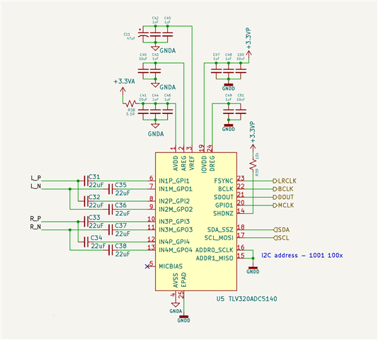
We're attempting to test TLV320ADC5140 in I2S master mode and by our understanding, supplying mclk was optional.  Out PCB has a pad for a single 24.576mhz crystal as we only operate in 48khz-related sample rates.  Currently, the XO is unpopulated.  Our understanding was that the TLV320 could supply its own internal BCK and LRCK outputs however given the sequence below we get no I2S BCK/LRCK.  Here is the schematic:

We attempted to activate with this sequence (pseudocode, using node.js and i2c library, registers are being written as confirmed below):

    const MST_CFG1_RATES = {
        48 : 0x48, // 01001000
        96 : 0x58, // 01011000
        192: 0x68, // 01101000
        384: 0x78 // 01111000
    };

    // SLEEP_CFG wake
    await i2cWriteByte(0x02, 0x91);

    // MST_CFG0 master, 48k 10000111
    await i2cWriteByte(0x13, 0x87);

    // i2cWriteByte(0x16, 0xXX); // CLK_SRC master (not using for now)

    // 256x 96k, 01011000
    await i2cWriteByte(0x14, MST_CFG1_RATES[96]);

    // ASI_CFG0 i2s, 32bit, 01110000 ? (not sure about last two bits)
    await i2cWriteByte(0x07, 0x70);

    // DSP_CFG sum pairs 00000100 ? not sure about HP
    await i2cWriteByte(0x6B, 0x04);

    // DEV_STS0 power up 1-4? 11110000
    await i2cWriteByte(0x76, 0xF0);

    // IN_CH_EN enable input 1-4? 11110000
    await i2cWriteByte(0x73, 0xF0);

    // ASI_OUT_CH_EN enable 1,2? 11000000
    await i2cWriteByte(0x74, 0xC0);

    // CH1_CFG0 config input, line, single-ended, no dre, 20k: 10101000
    await i2cWriteByte(0x3C, 0xA8);

    // CH2_CFG0
    await i2cWriteByte(0x41, 0xA8);

    // CH3_CFG0
    await i2cWriteByte(0x46, 0xA8);

    // CH4_CFG0
    await i2cWriteByte(0x4B, 0xA8);

Confirmed values with i2c read and got:

{
  '0x02': '10010001',
  '0x13': '10000111',
  '0x14': '1011000',
  '0x07': '1110000',
  '0x6B': '100',
  '0x76': '0',
  '0x73': '11110000'
}

0x76 does not seem set.  We still expected to see signs of life on FSYNC and BCLK.  Is the XO input required on GPIO1?  The datasheet made it seem optional so we wanted to test performance without it.  In addition, this I2S master is the master to our PCM5122 on the same board.  Haven't gotten that far, though.

  • Also FSYNC is 3.16V? That seems strange.

  • https://www.ti.com/lit/an/sbaa382/sbaa382.pdf?ts=1670883310063

    You need to feed an MCLK into GPIO 1. I include a snapshot from page 3 of the document

  • Update: Attached our XO at 24.576mhz and confirmed its waveform on the ADC GPIO1 pin.

    The problem now is that the I2S BCLK seems wrong and I'm not sure if it's due to the channel input situation.  We are using 4-into-2 mode.

    No matter what we've tried, getting LRCK/BCLK to come to life with PLL enabled seems impossible.

    This example from the tlv320ADC master mode doc got I2S to come to life but the desired BCLK also seems impossible to achieve:

    w 98 13 a0 # enable master mode, disable PLL for auto-clock config
    w 98 14 48 # FS = 44.1/48k BCLK/fsync ratio = 256
    w 98 16 d8 # MCLK is audio root, use MCLK_ratio_sel, MCLK/Fsync ratio = 512
    w 98 21 a0 # configure GPIO1 as MCLK input

    However, we still cannot get the LRCK/BCLK ratio to look right on the scope.  The XO on GPIO is 24.576mhz.  How would I get 96khz at 32 bit, 2 channels where ch1+2 is summed into LEFT and ch3-4 is summed into RIGHT?  All the combinations I try based on data sheet yield an incorrect BCLK.  It's easy to get the LRCK right...

    It's always been 6.144mhz.  32 bit * 96000 * 2 channels. 

    Can you please let us know if there's something we need to do because we're summing?

    Also very confused by this:

  • Can you or someone there tell me why this sequence would result in LRCK and SCLK being stuck high? Something isn't right.

        const i2c = i2cbus.openSync(BUS);
    
        // SLEEP_CFG wake // 10010001
        await i2cWriteByte(0x02, 0x91);
    
        /*
        this makes the device come to life, yes, but getting desired SCLK seems impossible
        w 98 13 a0 # enable master mode, disable PLL for auto-clock config
        w 98 14 48 # FS = 44.1/48k BCLK/fsync ratio = 256
        w 98 16 d8 # MCLK is audio root, use MCLK_ratio_sel, MCLK/Fsync ratio = 512
        w 98 21 a0 # configure GPIO1 as MCLK input
         */
         
        // back to enabling internal pll with MCLK supplied...now I2S is dead again
    
        // MST_CFG0 master, 48k 11100111
        await i2cWriteByte(0x13, 0x87); // was 0xe7
    
        // 256x 96k, 01011000 (5d, 8d)
        await i2cWriteByte(0x14, 0x58); // was MST_CFG1_RATES[96]
    
        // CLK_SRC master, use ratio (256) 11001000
        await i2cWriteByte(0x16, 0x10); // was 0xC8
    
        // set GPIO1 as MCLK input, 10100000
        // await i2cWriteByte(0x21, 0xa0);
    
        // ASI_CFG0 i2s, 32bit, 01110000 ? (not sure about last two bits)
        await i2cWriteByte(0x07, 0x70);
    
        // DSP_CFG sum pairs 00000100 ? not sure about HP
        await i2cWriteByte(0x6B, 0x04);
    
        // DEV_STS0 power up 1-4? 11110000
        await i2cWriteByte(0x76, 0xF0);
    
        // IN_CH_EN enable input 1-4? 11110000
        await i2cWriteByte(0x73, 0xF0);
    
        // ASI_OUT_CH_EN enable 1,2? 11000000
        await i2cWriteByte(0x74, 0xC0);
    
        // CH1_CFG0 config input, line, single-ended, no dre, 20k: 10101000
        await i2cWriteByte(0x3C, 0xA8);
    
        // CH2_CFG0
        await i2cWriteByte(0x41, 0xA8);
    
        // CH3_CFG0
        await i2cWriteByte(0x46, 0xA8);
    
        // CH4_CFG0
        await i2cWriteByte(0x4B, 0xA8);
    
        i2c.closeSync();

  • checking. shall revert by tomorrow

  • Can I also ask?  Something curious I found on github on a python driver someone wrote for this chip:

    #I2S CompatibilityWithZeroOffset(I2S only)
                #TLV320AICx140 devices can comply with the I2S bus format with zero offset by modifying
                # the default left justified format to fit the I2S format requirements, as follows:

    I've notice register 0x07 produces weird results either on or off but no clocks on FSYNC or BCLK.

    Somewhere else in e2e someone mentioned this but I can no longer find it.  Anyway, I still can't get the PLL enabled.

  • Here is where I left off after another whole day of attempts:

    w 4c 2 91 b10010001
    w 4c 13 97 b10010111
    w 4c 14 58 b1011000
    w 4c 21 a0 b10100000
    w 4c 7 be b10111110
    w 4c 6b 4 b100
    w 4c 76 f0 b11110000
    w 4c 73 f0 b11110000
    w 4c 74 c0 b11000000
    w 4c 3c a8 b10101000
    w 4c 41 a8 b10101000
    w 4c 46 a8 b10101000
    w 4c 4b a8 b10101000

    FSYNC/LRCK and BCLK are flat.  The only way I've gotten otherwise is to disable the pll.

  • Just to confirm we are still having ongoing issues getting any status on 0x15 other than a clock/ratio error.  Is there any other way to get help from TI?

  • I am sorry for the delay. i am taking a look at this and shall respond tomorrow

  • Sanjay, we got it working!  Thank you for your help. The problem was missing write to register PWR_CFG 0x75. This python driver is very helpful.

    I will post our exact sequence tomorrow morning in case someone else needs it in the future.  Now we just need to figure out the PCM5122 part.